Latest Manufacturing Technologies for 224Gbps High-Frequency Microwave Circuits (2026)
Shenzhen Hongda Circuit Technology Co., Ltd.
With the rapid development of data centers, 5G-Advanced, 6G pre-research, high-speed optical communication, and microwave radio frequency systems, the demand for ultra-high-speed, high-frequency, and high-reliability printed circuit boards (PCBs) is increasing exponentially. As a leading provider of high-end circuit board solutions, Shenzhen Hongda Circuit Technology Co., Ltd. has launched a full set of 2026 cutting-edge PCB manufacturing technologies for 224Gbps high-frequency microwave circuits, covering ultra-low-loss substrate systems, high-precision interconnection processing, signal integrity guarantee, multi-layer lamination process, co-packaged interconnection, intelligent manufacturing, thermal management, and reliability compliance. These technologies break through the technical bottlenecks of high-frequency signal attenuation, interconnection delay, and heat dissipation pressure in the 224Gbps PAM-4 transmission scenario, and provide core carrier support for next-generation high-speed interconnection products such as 3.2T optical modules, switch backplanes, and microwave radio frequency front-ends.
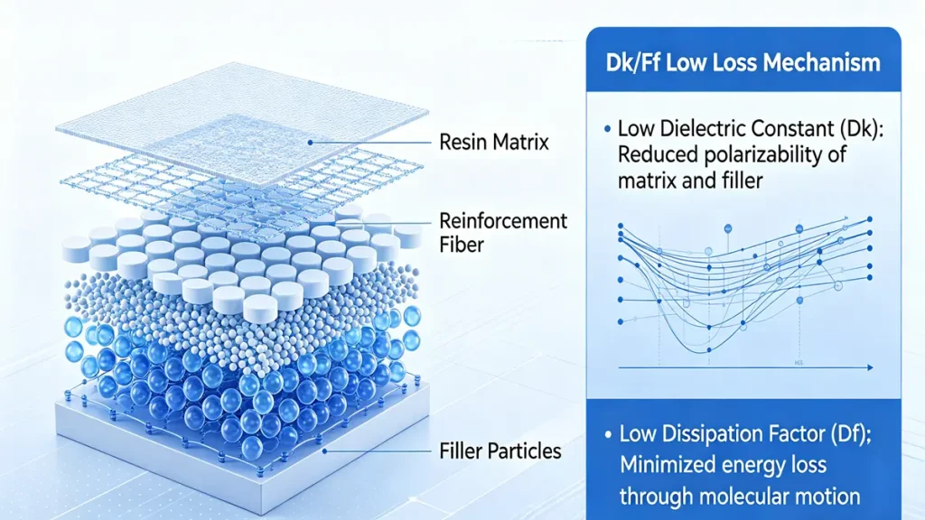
Ultra-Low-Loss Substrate Material Systems
The foundation of 224Gbps high-frequency transmission lies in low dielectric loss and stable electrical performance. In 2026, Hongda Circuit has fully upgraded its high-frequency substrate material system. The M9 grade high-frequency copper clad laminate (CCL) adopts hydrocarbon resin combined with high-purity quartz fiber cloth (Q-cloth) and HVLP4 ultra-low-profile copper foil. Its dielectric constant Dk is controlled at 2.8–3.2 (@10GHz), and dielectric loss factor Df is as low as 0.0005–0.0008 (@10GHz), with glass transition temperature Tg ≥200°C. Compared with the previous generation M8 material, the signal loss is reduced by 40%, which can stably support 224Gbps PAM-4 long-distance transmission. For higher-level 300Gbps and 3.2T interconnection needs, the company has deployed M10 next-generation high-performance substrates. This material achieves Df ≤0.0005, thermal expansion coefficient CTE <8ppm/°C, and the signal attenuation is controlled within 5% even at 300Gbps rate. It is specially optimized for 78–104 layers of ultra-high-layer PCB, and can meet the interconnection needs of large-capacity data center switches and core routing equipment. In addition, advanced PTFE and LCP composite materials are widely used in microwave and radio frequency modules. With their extremely low Dk/Df characteristics and excellent thermal stability, they ensure that the circuit has minimal signal loss and drift in complex high-frequency environments.
Advanced High-Density Interconnect (HDI) Fabrication
In 2026, Hongda Circuit’s high-density interconnection processing technology has reached the industry-leading level. The 7+ order Any-Layer HDI technology matched with micro-hole process realizes mass production of 50μm (0.05mm) laser micro-vias, with hole density exceeding 1000/cm², which greatly improves the wiring efficiency and integration of the circuit board. The substrate-like PCB (SLP) process is introduced to approach the packaging level of integrated circuits, realizing the highly integrated design of chip substrates and circuit boards, and effectively reducing the parasitic parameters and signal delay caused by interconnection. In terms of ultra-fine line manufacturing, the semi-additive process (SAP) is fully adopted, which stably produces 20μm line width and 15μm spacing, and has the technical reserve of sub-10μm line width/spacing, which can meet the wiring needs of high-frequency microwave circuits with extremely high integration. At the same time, 3D heterogeneous integration and TSV through-silicon via technology realize the vertical stacking of radio frequency, analog and digital functional layers, shorten the interconnection path, reduce signal crosstalk, and provide a process basis for the miniaturization and high performance of 224Gbps modules.
Precision Signal Integrity Engineering
Signal integrity is the core indicator of 224Gbps high-speed circuits. Hongda Circuit has built a full-chain precision signal integrity control system in 2026. The back-drilling technology achieves micron-level depth control, and the stub removal accuracy is within 100μm (4 mils), which completely eliminates the resonance problem caused by via stubs and ensures the purity of high-frequency signals. In the design and manufacturing of impedance-controlled transmission lines, the line width tolerance is controlled at ±0.5 mils, and the layer-to-layer alignment accuracy is ≤50μm (2 mils). It supports stripline, microstrip line, coplanar waveguide and other high-frequency transmission structures, and maintains stable impedance matching in the whole frequency band. In terms of surface treatment, ultra-smooth HVLP copper foil is used to reduce conductor loss at high frequencies; surface treatment processes such as ENEPIG, immersion silver and OSP are selected according to application scenarios, providing low-loss and high-reliability radio frequency contact surfaces, and avoiding signal reflection and attenuation caused by surface oxidation or poor contact.
Advanced Lamination & Stack-Up Technology
Aiming at the needs of high-speed backplanes and midplanes, Hongda Circuit has upgraded high-precision multi-layer lamination technology in 2026, supporting 28–104 layers of complex stack-up design, and adopting vacuum lamination with real-time pressure and temperature curve control to ensure the stability of interlayer bonding and electrical performance. In terms of thermal enhancement stack-up, embedded thermal vias and up to 10oz (350μm) heavy copper power layers are integrated to improve the current carrying capacity and heat dissipation efficiency of the circuit board. The integrated heat dissipation structure is designed for high-power microwave modules, which quickly conducts the heat generated by the chip and components to the outside, avoiding performance degradation or even failure caused by high temperature.
Co-Packaged & Near-ASIC Interconnect Solutions
To further reduce transmission loss, 2026 Hongda Circuit has launched co-packaged and near-ASIC interconnection solutions matching 224Gbps rate. Co-packaged copper (CPC) and co-packaged optics (CPO) technologies adopt on-substrate compression connectors to realize 224Gbps PAM-4 high-speed links, shorten the optical-electrical interconnection path, and reduce signal loss by more than 30% compared with traditional packaging. Near-packaged optics (NPO) further optimizes the layout of optical devices, making the signal path shorter and more stable. In terms of high-frequency connector and cable integration, it is matched with Samtec BE71A Bulls Eye® compression-mount test components (up to 71GHz) and phase-stable Nitrowave™ RF cables, which can complete accurate test and verification of 224Gbps PAM4 SerDes channels and ensure the consistency of product performance.
Intelligent Manufacturing & Quality Control
Intelligent manufacturing is an important guarantee for the stability of 224Gbps PCB mass production. In 2026, Hongda Circuit has built an AI-driven process control and digital twin system, which realizes real-time monitoring of key parameters such as lamination, etching and electroplating, and dynamically adjusts process parameters to ensure product consistency. Predictive maintenance technology is applied to 224Gbps special production lines to reduce downtime and improve production efficiency. In terms of testing and verification, 80GHz+ vector network analyzer (VNA) is used for S-parameter characterization to fully evaluate the high-frequency performance of the circuit. Automated optical inspection (AOI) and 224Gbps rate electrical testing realize full coverage of quality inspection, and eliminate defective products from the source.
Thermal Management Innovations
Aiming at the heat dissipation pressure of high-power 224Gbps modules, Hongda Circuit has innovated thermal management technology in 2026. Embedded liquid cooling channels are integrated into the PCB substrate, and micro-channel structures are used to achieve efficient liquid cooling heat dissipation, which can take away a lot of heat in a small space. At the same time, the thermal interface material (TIM) is optimized, and low thermal resistance TIM is selected to improve the heat transfer efficiency between components and the circuit board, forming a full-dimensional heat dissipation system from inside to outside.
Compliance & Reliability Standards
All 224Gbps high-frequency microwave circuit products of Hongda Circuit comply with CEI-224G-Linear and LPO-MSA industry standards, and are designed and manufactured in strict accordance with the specifications of 224Gbps interconnection. A number of extended reliability tests have been carried out, including thermal cycle, high temperature and high humidity, mechanical vibration and other tests, to adapt to the harsh working environment of telecom and data center equipment, and ensure the long-term stable operation of products for more than 10 years.
Relying on the above 2026 cutting-edge PCB manufacturing technologies, Shenzhen Hongda Circuit Technology Co., Ltd. continues to lead the innovation of high-speed high-frequency circuit boards, providing safe, reliable, high-performance carrier solutions for global 224Gbps and even higher rate interconnection systems, and empowering the rapid development of next-generation information and communication infrastructure.