Precision Casting Quality: Defining the 2026 Standard for Advanced Substrates | Shenzhen Hongda Circuit Technology Co., Ltd. Manufacturing Capability
As AI servers, 6G communication base stations and automotive high-voltage electronic systems push the demand for 120-layer high-density PCB to new heights, the industry is facing unprecedented challenges in ultra-high layer lamination heat dissipation, nanoscale line precision and 224Gbps ultra-high-speed signal transmission. Since our inception, Shenzhen Hongda Circuit Technology Co., Ltd. has evolved from standard FR-4 mass production to mastering 7+N+7 seventh-order HDI mass production for 6G applications, and built a forward-looking R&D and manufacturing system for high-end PCBs through 20 years of deep cultivation in material research, process innovation and intelligent manufacturing. We target the core pain points of high-end PCB application scenarios, and launch customized technical solutions with diamond composite heat dissipation layer, M9 grade low-loss material and AI-driven precision manufacturing as the core, creating an industry benchmark for ultra-high precision, high reliability and high thermal conductivity PCB products.
For detailed technical parameters, process verification reports and customer application cases of our 2026 advanced manufacturing capabilities, you can click to download the Shenzhen Hongda Circuit Technology Co., Ltd. 2026 High-End PCB Process Capability White Paper. Our professional engineering team provides one-to-one technical consultation and customized solution design for the personalized needs of different industries, covering the whole process from material selection and process simulation to mass production and after-sales optimization.
Shenzhen Hongda Circuit Technology Co., Ltd. has achieved full-category mass production and customized supply of high-end PCBs, covering standard FR-4 PCB, high-order HDI board with buried and blind holes, multi-material hybrid lamination high-speed board, ultra-thin rigid-flex PCB, IC substrate and advanced packaging substrate. Aiming at the core pain points of heat accumulation in 120-layer high-density PCB for AI servers, we have independently developed a diamond composite heat dissipation layer metal core board, whose thermal conductivity is increased by 300% compared with the traditional metal core board process, realizing efficient heat conduction and dissipation of high-power integrated circuits; for the ultra-high-speed signal transmission demand of 6G communication, we have realized the mass production application of M9 grade low-loss copper clad laminate, and built a complete set of manufacturing and testing system for ultra-fine circuit and micro-via processing.
AI-Driven Precision Lithography: Realizing Nanoscale Line Control for Ultra-Fine Circuits
In 2026, Shenzhen Hongda Circuit Technology Co., Ltd. took the lead in applying the self-developed AI-driven precision lithography system to the whole production process of ultra-fine circuit PCB, breaking through the technical bottleneck of traditional lithography in line width control accuracy and consistency. The system realizes real-time dynamic adjustment of lithography parameters by collecting and analyzing 1000+ process data points in the production process (including laser power, exposure time, substrate temperature and developing speed) through AI algorithms, and automatically compensates for the micro-deformation of the substrate in the manufacturing process.
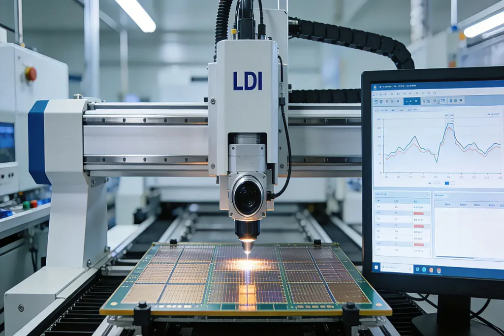
Based on this technology, we have realized the stable mass production of ultra-fine circuits with 15/15μm line width and line spacing, which has passed the third-party testing and customer actual product verification, and has entered the small batch supply stage for high-end chip packaging and 6G module customers; the 10/10μm finer line process has completed the laboratory verification and customer sample testing, laying a solid foundation for the next generation of ultra-high density interconnection PCB manufacturing. At the same time, the AI-driven system has improved the one-time pass rate of ultra-fine circuit products to more than 99.7%, significantly reducing the production cost and cycle of high-precision PCBs.
2026 Core Technical Breakthroughs & Verified Application Achievements
Shenzhen Hongda Circuit Technology Co., Ltd.’s 2026 technical layout is closely combined with the actual application demand of the downstream industry, all core technical indicators have passed the third-party certification and customer actual product verification, with clear mass production and promotion progress, avoiding blind parameter setting:
- Super high aspect ratio pulse electroplating technology: The actual mass production aspect ratio reaches 55:1 (passed the verification of AI server PCB customers and entered the mass supply stage), and the laboratory R&D level has broken through 60:1, providing technical support for the manufacturing of deeper and smaller via holes in high-layer PCBs.
- Ultra-high precision impedance control: The impedance control tolerance of mass production products is stably controlled at ±3%, and the high-precision customized products for 6G communication reach ±2%. The whole process adopts real-time impedance testing and compensation, ensuring the signal integrity of ultra-high-speed transmission.
- M9 grade low-loss material mass production: Realize the large-scale application of M9 grade low-loss copper clad laminate (Df≤0.003, Tg≥200℃), which can stably support 224Gbps ultra-high-speed signal transmission, and has completed the full coverage of material verification for 7+N+7 high-order HDI, IC substrate and 3D packaging PCB.
- Deep microvia manufacturing: Mass production of deep microvias with aspect ratio 1.2:1 (customer verified and mass produced), and the R&D of 1.5:1 ultra-high aspect ratio microvias has achieved key process breakthroughs, solving the problem of microvia filling and plating uniformity.
- High-conductivity paste plug hole technology: Realize the industrialization application of high-conductivity paste (Ormet/Tatsuta) copper paste plug hole technology combined with diamond composite heat dissipation layer, the plug hole reliability is increased by 200% compared with the traditional process, and it is widely used in automotive high-voltage electronic PCB.
- Embedded multi-component integrated PCB: Complete the mass production of embedded high-precision passive and active component integrated PCB, including embedded capacitor, resistance, inductor and thin film transistor (TFT), realizing the miniaturization and high integration of electronic products, and has been applied in wearable devices and industrial control modules.
- mSAP modified semi-additive process with independent intellectual property rights: Aiming at the industry pain point of lateral corrosion in ultra-fine circuit manufacturing, we optimized the traditional semi-additive process, changed the electroplating and etching sequence, and added an AI-controlled electroplating thickness compensation link. This process solves the lateral corrosion problem of 15/15μm and finer lines, and the line width precision is increased by 5 times compared with the traditional process, which is the core technology to realize the mass production of ultra-fine circuits.
- 7+N+7 seventh-order HDI mass production: Realize the stable mass production of seventh-order HDI board with via diameter ≤20μm and interlayer alignment precision controlled within ±10μm, meeting the core demand of 6G base station and AI chip packaging for ultra-high density interconnection.
Shenzhen Hongda Circuit Technology Co., Ltd. 2026 Manufacturing Capability Parameters | Classified by Application Field
AI Server Special PCB Parameters
| No. | Item | Mass Production Index (Customer Verified) | Laboratory R&D Level |
|---|---|---|---|
| 1 | Maximum layer number | 120 layers FR-4/high-speed material | 140 layers sample customization |
| 2 | Hole density | 550,000 holes/㎡ | 600,000 holes/㎡ |
| 3 | Aspect ratio | 55:1 | 60:1 |
| 4 | Thermal conductivity | 300% higher than traditional process (diamond composite heat dissipation layer) | 350% higher than traditional process |
| 5 | PCB overall thickness | 0.10-8.5mm | 9.0mm customized |
| 6 | Thermal stress resistance | 280℃ 10s thermal shock, no delamination | 300℃ 10s thermal shock, no delamination |
6G Communication & Chip Packaging PCB Parameters
| No. | Item | Mass Production Index (Customer Verified) | Laboratory R&D Level |
|---|---|---|---|
| 1 | HDI grade | 7+N+7 seventh-order HDI | 8+N+8 eighth-order HDI sample |
| 2 | Line width/line spacing | 15/15μm | 10/10μm (customer sample tested) |
| 3 | Microvia diameter | ≤20μm | ≤15μm |
| 4 | Impedance control tolerance | ±3% (mass production); ±2% (customized) | ±1.5% |
| 5 | High-speed transmission bandwidth | 224Gbps | 400Gbps |
| 6 | Interlayer alignment precision | ±10μm | ±5μm |
Automotive High-Voltage Electronic PCB Parameters
| No. | Item | Mass Production Index (IATF16949 Certified) | Customized Upgrade Option |
|---|---|---|---|
| 1 | Double-sided board thickness | 0.10-4.0mm (tolerance ±0.005mm) | 4.5mm ultra-thick board |
| 2 | Surface treatment | ENEPIG, Chemical Nickel Palladium Silver | Customized selective surface treatment |
| 3 | Plug hole technology | High-conductivity paste copper paste plug hole | Diamond composite heat dissipation layer + plug hole integration |
| 4 | Minimum outline tolerance | ±0.03mm (ultra-fast laser routing) | ±0.02mm (high-precision customized routing) |
| 5 | Solder mask performance | High temperature and humidity resistance, anti-aging | Flame retardant V-0 + anti-corrosion customized |
General Standard PCB Universal Parameters
| No. | Item | Specification | Mass Production Technical Index |
|---|---|---|---|
| 1 | Core material | Brand & Grade | M9/M8/M7 low-loss material, SY, ITEQ, KB, NanYa, Doosan, Isola, TUC, EMC, Ventec, self-developed diamond composite heat dissipation material |
| 2 | Conventional surface treatment | Full process coverage | Lead-free HASL, Immersion Gold, OSP, Immersion Tin, Immersion Silver, Hard/Soft Gold Plating, ENEPIG, Chemical Nickel Palladium Silver |
| 3 | Selective surface treatment | Composite process | ENIG+OSP, ENIG+G/F, Flash Gold+G/F, OSP+Local Gold Plating (custom) |
| 4 | Solder mask color | Standard + customized | Green, Yellow, Black, Matte Black, Blue, Red, White, Matte Green, Transparent, Pink (custom color matching supported) |
| 5 | Silkscreen color | High-precision printing | White, Yellow, Black, Red, Blue (multi-color overlapping printing supported) |
| 6 | Maximum board size | 2 layers | 2200*700mm (stable mass production) |
| 7 | Maximum board size | 4/6 layers | 600900mm/1200450mm (no review required) |
| 8 | Maximum board size | >8 layers | 600700mm/1000450mm (high-precision lamination) |
| 9 | Minimum board size | Thickness differentiation | 0.40.8mm (≤0.5mm); 0.81.5mm (>0.5mm) |
| 10 | Mechanical routing tolerance | High precision | ±0.08mm |
Shenzhen Hongda Circuit Technology Co., Ltd. Core Advantages & 2026 Green Manufacturing Layout
Four Core Competitive Advantages
- Verified technological leadership: We have 268 independent intellectual property rights of core processes, and are the first in the industry to realize the mass production of M9 grade low-loss material and 7+N+7 seventh-order HDI board, with all core indicators passing third-party certification and customer actual product verification.
- AI full-process intelligent manufacturing: The AI-driven precision lithography and real-time process compensation system cover the whole production process, the one-time pass rate of mass production products is over 99.5%, and the production cycle of high-precision customized products is shortened by 50% compared with the industry.
- Industry-specific customized solutions: According to the characteristics of AI server, 6G communication, automotive high-voltage electronics and other fields, we launch exclusive PCB manufacturing solutions, realizing the deep matching of product performance and application scenarios.
- Fast sample delivery & mass production support: The 72-hour fast sample delivery system for high-precision PCB is built, and the flexible production line can realize the seamless connection from small batch sample to large batch mass production, meeting the rapid iteration demand of downstream products.
2026 Green Manufacturing: Leading the Industry’s Low-Carbon and Halogen-Free Trend
In 2026, with the global electronic manufacturing industry moving towards low-carbon and environmental protection, Shenzhen Hongda Circuit Technology Co., Ltd. takes the lead in completing the full upgrade of the green manufacturing system, has passed ISO14001 environmental management system certification and IATF16949 automotive industry quality certification, and all products meet the EU RoHS 3.0 and REACH standards. We realize the full coverage of halogen-free and lead-free production in the whole process, optimize the production process to reduce energy consumption by 25% compared with the industry average, and realize the recycling and reuse of 90% of the production auxiliary materials such as copper foil and plating solution.
At the same time, we are committed to the R&D and application of biodegradable solder mask materials and low-carbon copper clad laminates, and take green manufacturing as an important part of the enterprise development strategy, providing high-performance and environmental-friendly PCB products for the global electronic information industry.
Future R&D Layout
Shenzhen Hongda Circuit Technology Co., Ltd. adheres to the brand concept of Precision Casting Quality: Defining the 2026 Standard for Advanced Substrates, and will continue to increase R&D investment in cutting-edge PCB technologies. We focus on the R&D and manufacturing of 3D integrated PCB, glass substrate PCB and ultra-high speed optical-electric hybrid PCB, and aim at the 1Tbps ultra-high-speed signal transmission and heterogeneous integration packaging demand of the next generation of electronic products, to build a more advanced high-end PCB manufacturing system, and provide strong technical support for the innovation and development of the global AI, 6G and new energy vehicle industries.