Standard Process
Minimum Line/Spacing (Internal/External Layers): 0.002”/0.002” (50μm/50μm)
Ultra-Fine HDI: 2.5/2.5 mil (63.5μm/63.5μm) with controlled-impedance etching
Etch Profile Factor: ≥2.0 for consistent trace sidewalls
Laser Microvia Diameter: 50μm (advanced), 75–150μm (standard)
Mechanical Drill Min. Size: 0.003” (75μm)
Microvia Aspect Ratio: ≤0.75:1
Through-Hole Aspect Ratio: Up to 20:1
Laser Drilling Alignment: ±10μm
Max Layer Count: 120 layers (any-layer HDI)
Stackup Configurations: 4+N+4 buildup, 7-stage HDI, rigid-flex hybrid
Layer-to-Layer Registration: ±25μm
Impedance Tolerance: ±5% (50Ω single-ended, 100Ω differential)
Max Signal Speed: 120Gbps+ (Megron 8 materials)
Material Dk/Df: M9-grade (Dk≤3.2, Df≤0.0008) for AI/HPC
Product Details
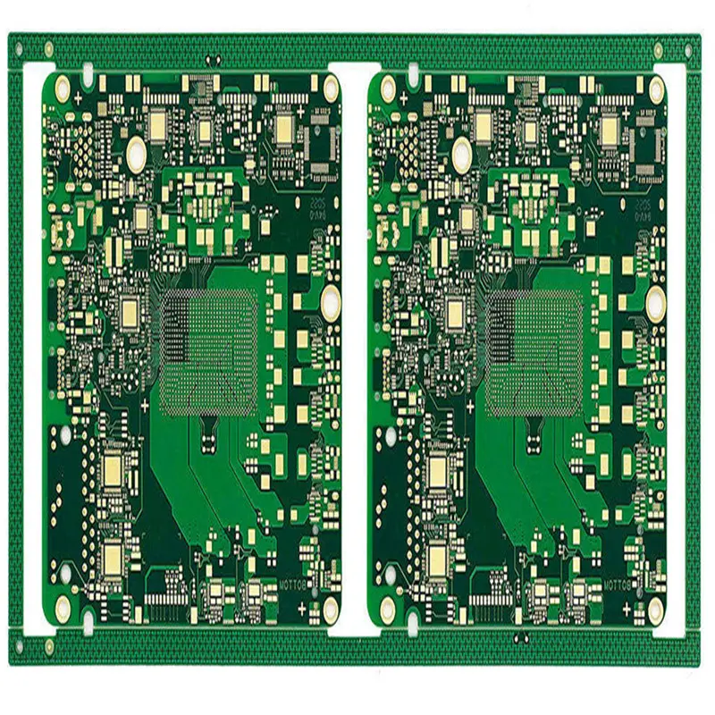
High-Precision HDI PCB Solutions: 120-Layer Capability & 5μm Microvia Technology
Core Selling Points & Technical Positioning
As the core carrier of high-end electronic equipment, High-Density Interconnect (HDI) PCBs are crucial for realizing miniaturization, high performance, and high-speed signal transmission. Hongda Circuit stands at the top tier of the industry, focusing on providing high-precision and reliable HDI PCB solutions for professional engineers and purchasers worldwide. Our core competitiveness lies in our 120-layer manufacturing capability and 7-tier HDI blind/buried via technology, which perfectly address the core demands of high-end electronic products for precision interconnection and signal stability. With advanced manufacturing processes and strict quality control, we are committed to becoming a trusted partner for global customers in the fields of 5G/6G, AI computing, automotive electronics, and aerospace.
Technical Specifications
The technical specifications are the soul of HDI PCBs, reflecting our manufacturing precision and process capabilities. All indicators are standardized and data-driven to ensure transparency and reliability.
| Items | Hongda Circuit Technical Standard |
|---|---|
| HDI Stack-up | 1+N+1, 2+N+2 up to Any-layer (Any-layer Interconnection) |
| Min Microvia | 5μm |
| Min Trace/Space | 10μm / 10μm |
| Impedance Control | ±5% (Adopting AI Real-time Compensation Technology) |
| Layer Count | Up to 120 Layers |
| Surface Finish | ENIG (Electroless Nickel Immersion Gold), ENEPIG (Electroless Nickel Electroless Palladium Immersion Gold), OSP, Immersion Silver |
Technical Highlights
We focus on breaking through the technical difficulties of HDI PCBs, and each technical advantage is designed to enhance product performance and meet the evolving needs of high-end applications.
Microvia Expertise
We specialize in microvia technology, supporting 5μm microvias and an aspect ratio of up to 100:1. The ultra-small microvia design effectively reduces parasitic inductance and capacitance, minimizes signal crosstalk, and significantly improves signal integrity—critical for high-speed and high-frequency applications. Leveraging advanced laser drilling technology and precise alignment control, we ensure the uniformity and reliability of each microvia, laying a solid foundation for the stable operation of high-end electronic devices. This technology also aligns with the industry trend of miniaturization, enabling more compact and integrated module designs.
Ultra-Fine Circuitry
Adopting the mSAP (Modified Semi-Additive Process), we achieve 10μm-level fine wiring, which is far beyond the capabilities of traditional PCB manufacturing processes. The mSAP process reduces lateral corrosion during circuit etching, ensuring the accuracy and consistency of line width and line spacing, and effectively improving the density of circuit layout. This technology perfectly meets the miniaturization and high-integration needs of 5G/6G modules, AI chips, and high-end consumer electronics, and is also compatible with the emerging CoWoP (Chip on Wafer on PCB) packaging technology, enabling seamless integration of chips and PCBs.
Advanced Substrate Solutions
To address the challenges of signal loss and skin effect in high-speed transmission scenarios up to 224Gbps, we adopt M9-grade ultra-low loss substrates and VLP2 (Very Low Profile) copper foil. The M9 substrate features an ultra-low dielectric loss (Df < 0.002) and stable dielectric constant (Dk ≈ 2.8-3.1), which effectively reduces signal attenuation during high-frequency transmission. The VLP2 copper foil minimizes surface roughness, reducing skin effect and signal loss, ensuring the stability and integrity of high-speed signals. This substrate solution has passed relevant certifications and is widely used in high-end AI servers and high-speed optical modules, matching the technical requirements of NVIDIA GB300 series chips.
Key Applications
With rich industry experience and mature manufacturing capabilities, our HDI PCBs have been widely applied in various high-end fields, providing reliable support for the innovation and development of downstream industries. We have in-depth cooperation with global leading enterprises, accumulating a wealth of application cases and technical experience.
Consumer Electronics
Our HDI PCBs are widely used in high-end smartphones, wearable devices (smart watches, VR/AR headsets), and 5G modules. The ultra-fine circuitry and high-density interconnection capabilities enable the miniaturization and multi-functionality of consumer electronic products, improving product performance and user experience. As AI phones and AI PCs gain popularity, our HDI solutions also support the evolution of motherboards to 8-12 layers, meeting higher performance requirements.
Communications & Computing
In the field of communications and computing, our HDI PCBs are applied in 224Gbps high-speed servers, AI computing cards, and 800G optical modules. With excellent signal integrity and high-temperature resistance, they ensure the stable operation of high-speed data transmission and large-scale computing. As AI servers become a key growth driver, our 18-layer+ high-order HDI boards have been widely used in GPU accelerator modules, accounting for a significant share of the global market.
Automotive & Aerospace
In the automotive and aerospace fields, our HDI PCBs are used in 77GHz/79GHz millimeter-wave radars, autonomous driving domain controllers, and satellite communication equipment. We adhere to strict quality standards to ensure that products can withstand harsh working environments such as high temperature, high humidity, and strong vibration, providing reliable interconnection solutions for automotive intelligence and aerospace engineering. With the rapid development of new energy vehicles, the demand for HDI in automotive electronics is growing rapidly, and our products have been recognized by many leading automotive manufacturers.
Quality Assurance
For high-value HDI PCBs, quality is the cornerstone of trust. We have established a full-process quality control system, from raw material procurement to finished product delivery, to ensure that each PCB meets international standards and customer requirements.
Certification System
We have obtained a number of international authoritative certifications, including ISO 13485 (medical industry), ISO 9001 (quality management system), and UL certification. These certifications fully demonstrate our strict quality management capabilities and product reliability, enabling our products to enter global markets smoothly and meet the quality requirements of various high-end industries.
Testing Technology
We adopt AOI (Automated Optical Inspection) + X-Ray integrated detection technology, combining the advantages of visual inspection and internal detection to achieve full coverage of product defects. The detection system can accurately identify microvia alignment errors, circuit short circuits, and other defects, ensuring a defect detection rate of ≥99.9%. With advanced X-Ray drilling target machines, we achieve layer alignment accuracy within ±1μm, far exceeding the industry average, and ensuring the reliability of interlayer interconnection.
Digital Twin
We introduce digital twin technology to realize full-link digital monitoring of the entire manufacturing process. From design, material selection, and production to testing, each link is digitized and recorded, ensuring that each PCB has complete traceability. This technology not only improves production efficiency but also enables real-time monitoring and adjustment of production parameters, effectively reducing production defects and ensuring stable product quality.
Call to Action
Need a quote for your complex HDI design? Upload your Gerber files for a professional DFM (Design for Manufacturability) audit. Our team of senior RF and high-speed signal engineers will provide you with professional impedance simulation and stack-up optimization suggestions before manufacturing, helping you reduce design risks, improve production efficiency, and lower manufacturing costs. We are committed to providing customized solutions according to your specific needs, supporting your product innovation and market competition.
HDI in the 6G Era: Technical Outlook
As the global 6G technology enters the critical stage of research and development and industrial cultivation, HDI PCBs will become a core supporting component for 6G infrastructure. 6G technology aims to achieve global coverage of air, space, land, and sea, as well as in-depth integration of computing power and networks, which puts forward higher requirements for the interconnection density, signal transmission speed, and reliability of PCBs. Our HDI solutions, with 5μm microvia technology, 120-layer manufacturing capability, and AI-driven precision compensation technology, can perfectly meet the needs of 6G for high-frequency, high-speed, and miniaturized interconnection. The AI real-time impedance compensation technology we adopt can dynamically adjust production parameters according to the characteristics of 6G high-frequency signals, effectively solving the problem of signal loss in 6G transmission and providing strong technical support for the commercialization of 6G technology. We will continue to increase R&D investment, keep pace with the evolution of 6G technology, and maintain our leading position in the high-end HDI field.