Standard Process
Layer Count: 30+ layers mass production, any-order HDI supported Copper Foil: HVLP4-grade 3μm ultra-thin copper foil, Rz ≤ 0.5μm Substrate: M9-grade hydrocarbon resin with ≥99.995% high-purity quartz cloth CTE: ≤14ppm/℃ Dielectric: Dk 2.2–2.5, Df ≤ 0.0005 @100GHz Fine Line: mSAP process, 1.5mil/1.5mil L/S in mass production Impedance Control: ±2% high precision Interconnection: 0.2–0.5mm laser micro-vias, density ↑≥300% Signal Delay: Sync error ≤0.5ns Thermal Conductivity: ≥2.5W/(m·K), VC integrated Thermal Stability: Tg ≥200℃, UL94-V0 approved EMI Shielding: Nano-coating, suppression ≥95% Dimensional Tolerance: ±2μm for core thickness & resin content Inspection: 3D AOI + big data, nanoscale defect detection Quality: 100% defect detection rate, false alarm <0.1% Compliance: 5G-A/6G & AI data center EMC certified Ultra-Thin: 0.05–0.1mm for wearable & foldable devices Flex Performance: Dynamic flex >10,000,000 cycles; folding radius <1mm, >200,000 cycles Rigid-Flex: 2–14 layers
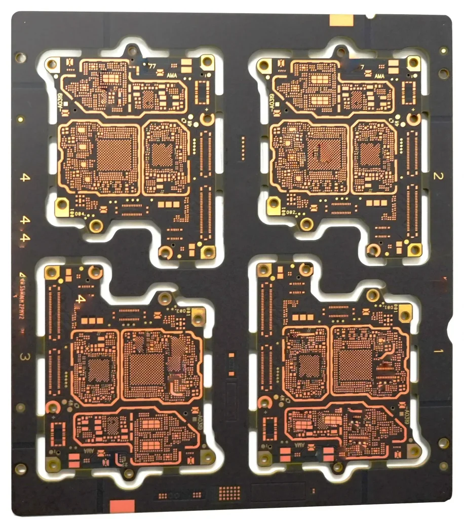
Product Details
What is 2026 New Generation High Speed PCB?
With the explosive growth of AI computing power and the pre-research and development of 6G communication technology, the definition of high-speed circuit has been fully upgraded in 2026. A circuit is defined as a high-speed circuit when the frequency of digital logic circuit reaches or exceeds 100MHz, and the high-speed circuit accounts for more than 50% of the entire electronic system.
The new generation of high-speed PCB is the core interconnection carrier of high-frequency and high-density electronic systems, manufactured by integrating 2026 global leading material technology and ultra-precise manufacturing process. It realizes the dual breakthrough of ultra-low loss signal transmission and three-dimensional high-density integration, and is the core hardware foundation for supporting AI server high computing power operation, 1.6T optical module ultra-high speed data transmission and 5G-A/6G communication signal processing.
Different from the traditional high-speed PCB, the 2026 version of high-speed PCB takes signal integrity, power integrity and thermal integrity as the core design principles, and solves the industry pain points of high-frequency signal attenuation, high-density heat accumulation and ultra-precise impedance control in high-load operation scenarios.
2026 High Speed PCB Material Selection Criteria & Core Upgrades
Shenzhen Hongda Circuit Technology Co., Ltd. adheres to the “extreme performance + scenario customization” material selection concept, and on the basis of the classic low-loss and high-stability requirements, combines the 2026 industry demand of AI high computing power and 6G pre-research, and upgrades the high-speed PCB material selection criteria to 7 core requirements, all of which target the technical bottlenecks of high-end high-speed PCB application:
- Ultra-low loss performance: Df ≤ 0.0005 at high frequency (100GHz), with excellent CAF resistance, ultra-high temperature resistance (Tg ≥ 200℃) and mechanical toughness, to meet the long-term stable operation of high-load equipment
- Ultra-stable Dk/DF parameters: The variation coefficient with frequency (0-100GHz) and temperature (-40~125℃) is less than 0.05, fundamentally suppressing signal dispersion and impedance mutation
- Nanoscale material tolerance: The tolerance of core material thickness and glue content is controlled within ±2μm, realizing picometer-level impedance matching control and meeting the ultra-precise requirement of 1.6T optical module
- Extreme smoothness of copper foil: HVLP4 grade copper foil with surface roughness Rz ≤ 0.5μm, eliminating the signal loss caused by skin effect in ultra-high frequency transmission; at the same time, the vacuum sputtering process ensures high peel strength while low roughness
- High-performance glass fiber cloth/quartz cloth: Priority selection of low-CTE electronic cloth or high-purity quartz cloth (purity ≥99.995%), with flat window structure, reducing signal skew and loss by more than 40% compared with traditional glass cloth
- Thermal conductivity matching: The thermal conductivity of the substrate is ≥ 2.5W/(m·K), realizing the synergy of signal transmission and heat dissipation, solving the problem of material deformation caused by high heat accumulation of AI server
- High-rigidity anti-deformation: For 30+ layer high-multilayer PCB, the material is required to have high flexural modulus and low thermal expansion coefficient (CTE ≤14ppm/℃), avoiding layer separation and warpage in the manufacturing and use process
Core Parameter Impact & 2026 Technical Breakthrough
The signal integrity of the new generation high-speed PCB is jointly determined by impedance consistency, transmission line ultra-low loss, time delay synchronization and thermal stability. The key parameters Dk and Df are still the core of material selection, but the index requirements have been comprehensively upgraded in 2026:
- Dielectric constant (Dk): The optimal value is controlled at 2.2~3.4 (12GHz). The ultra-stable Dk value avoids the impedance mutation caused by frequency and temperature changes, and fundamentally eliminates the harmonic component loss and frequency offset of 224Gbps high-speed signals. Especially for quartz cloth materials, the Dk value can be as low as 2.2 at high frequency, which is the first choice for 6G pre-research equipment.
- Dispersion suppression: Based on the new M9 grade carbon hydrogen resin system and high-purity quartz cloth, the Dk value variation with frequency is reduced to the minimum, and the dispersion caused by dielectric polarization, material loss and copper foil roughness is completely suppressed.
- Loss system optimization: The 2026 generation high-speed PCB loss is divided into dielectric loss, conductor loss, radiation loss and thermal loss. Shenzhen Hongda Circuit Technology Co., Ltd. has realized the whole link loss control through material compounding and process optimization, and the total transmission loss is reduced by more than 50% compared with the traditional high-speed PCB.
2026 Key Material Upgrade & Classification System
FR4 is still the basic resin system of high-speed PCB, but in 2026, it has completed the iteration from general grade to ultra-low loss high-performance grade. The new generation FR4 is based on modified epoxy resin/carbon hydrogen resin, combined with HVLP4 grade copper foil, quartz cloth and other core materials, and has become the mainstream material of mid-to-high end high-speed PCB. Shenzhen Hongda Circuit Technology Co., Ltd. has built a complete high-speed PCB material classification system according to the 2026 industry development trend, covering all application scenarios of high-speed electronic systems:
- Classification by glass fiber cloth/quartz cloth type: On the basis of traditional 106/2116/7628 glass fiber cloth, add low-CTE electronic cloth, high-purity quartz cloth (Q cloth) and ultra-low loss electronic cloth, among which quartz cloth has become the core material for AI server 30+ layer PCB and 6G pre-research equipment due to its ultra-low Dk and ultra-low loss characteristics
- Classification by glass type: E-glass (basic grade) + NE-glass (low-Dk grade) + quartz glass (ultra-high performance grade). In 2026, the application proportion of NE-glass and quartz glass in Shenzhen Hongda Circuit Technology Co., Ltd. high-speed PCB has exceeded 70%, realizing the comprehensive upgrade of material performance
- Core material system of mainstream suppliers (2026 upgraded version):
- Iteq: IT988GSE/IT968SE (Low-Dk special grade for optical module)
- Tuc: Tu872SLK-SP/Tu933+ (high thermal conductivity grade for AI server)
- Panasonic: Megtron7/M8/M9 (AI server exclusive high-performance grade)
- Shenzhen Hongda Circuit Technology Co., Ltd. Custom: M9 grade low-loss composite material (self-developed, for 1.6T optical module and 6G pre-research)
- Rogers: RO4350B/RO4835 (RF/6G pre-research special grade)
- Classification by loss level (2026 new industry standard): Ultra-low loss sheet (Df < 0.001), low loss sheet (0.001 ≤ Df < 0.005), medium loss sheet (0.005 ≤ Df < 0.02), general loss sheet (Df ≥ 0.02)
- Flame retardant grade: UL94-V0 is the standard configuration, and customized UL94-V0 high-temperature resistant grade (150℃ long-term operation) is available for high-heat equipment such as AI server, matching the high-temperature operation environment of high computing power chips
- Substrate type classification: Traditional organic substrate + glass substrate (2026 breakthrough technology). Glass substrate solves the problems of high heat deformation and signal attenuation of traditional organic materials, and is the core material for the next generation of high-speed PCB
2026 Latest Manufacturing Technology of High Speed PCB – Shenzhen Hongda Circuit Technology Co., Ltd. Core Technological Breakthrough
In 2026, Shenzhen Hongda Circuit Technology Co., Ltd. integrated the global latest PCB manufacturing technology and independent R&D achievements, realized the technological breakthrough of high integration, ultra-precision and high stability in high-speed PCB production, breaking the technical bottleneck of traditional high-speed PCB in AI and 5G-A/6G application. The core process upgrades include the following 8 key technologies, all of which have achieved mass production application:
1. HVLP4 Grade Ultra-thin Carrier Copper Foil Mass Production Technology
Realize the mass application of 3μm ultra-thin carrier copper foil with independent intellectual property rights, and match the HVLP4 grade surface treatment with Rz ≤ 0.5μm. Through the vacuum sputtering + nano-level electroplating composite process, solve the problem of low peel strength caused by low roughness, and maintain the peel strength at more than 0.8kN/m while the surface is extremely smooth, fundamentally reducing the conductor loss caused by skin effect in ultra-high frequency transmission, which is the core process of AI server high-speed signal transmission.
2. 30+ Layer High Multi-layer & Any-order HDI Integration Technology
Aim at the high computing power demand of AI server, realize the stable mass production of 30+ layer high-speed PCB, and match the any-order HDI technology. The ultra-precise laser micro-via drilling realizes the micro-via processing of 0.2~0.5mm diameter, and the interconnection density is increased by more than 3 times compared with the traditional process, realizing the miniaturization and three-dimensional high integration of AI server PCB, replacing the traditional copper cable connection with PCB interconnection, reducing the signal delay by more than 60%.
3. Laser Direct Imaging (LDI) + Modified Semi-additive Process (MSAP)
Abandon the traditional subtractive etching process, adopt the upgraded MSAP process matched with high-precision LDI, realize the 1.5mil/1.5mil ultra-fine line/spacing mass manufacturing, the line wall straightness is ≥99%, and the impedance control accuracy is ±2%, which meets the ultra-precise wiring demand of 1.6T optical module and 6G pre-research equipment.
4. Glass Substrate Lamination & Low-CTE Material Synergy Technology
As the core breakthrough technology of PCB industry in 2026, Shenzhen Hongda Circuit Technology Co., Ltd. has realized the mass production application of glass substrate lamination technology. Glass substrate solves the problems of high heat deformation and signal attenuation of traditional organic materials, and is matched with low-CTE electronic cloth (thermal expansion coefficient ≤14ppm/℃) and high thermal conductivity substrate. The integrated design of heat conduction copper foil + VC heat equalizing plate controls the high-load operation temperature of PCB within 80℃, completely solving the problems of copper foil peeling, material shrinkage and warpage caused by high heat accumulation of high-density equipment.
5. M9 Grade Carbon Hydrogen Resin & Quartz Cloth Lamination Technology
For 6G pre-research and ultra-high frequency RF equipment, adopt the latest M9 grade carbon hydrogen resin + high-purity quartz cloth lamination technology in 2026. The quartz cloth with purity ≥99.995% makes the Dk value stable at 2.2~2.5, Df ≤ 0.0005, and the radiation loss is reduced by more than 60% compared with the traditional material, which is the core process of Shenzhen Hongda Circuit Technology Co., Ltd.’s 6G pre-research high-speed PCB.
6. AI-driven Full-process Impedance Matching & Layout Optimization
Introduce the self-developed AI high-speed PCB design algorithm into the whole process of design and manufacturing, realize the intelligent optimization of impedance matching and wiring layout, and the time delay synchronization error of multi-channel high-speed signal is controlled within 0.5ns. Through the AI simulation of signal transmission path, fundamentally solve the problems of crosstalk and parasitic capacitance in high-density layout, and improve the design efficiency by more than 80%.
7. 3D AOI + In-situ Detection + Big Data Defect Analysis
Upgrade from traditional 2D AOI to 3D AOI + in-situ detection + big data defect analysis full-process quality control system, realize the nanoscale defect detection of copper surface, via and line, the defect detection rate is 100%, and the false detection rate is less than 0.1%. By analyzing the defect big data, optimize the production process in real time, eliminating the signal degradation risk caused by manufacturing defects.
8. Anti-EMI Integrated Shielding & Nano Coating Technology
Adopt the customized anti-EMI high-temperature resistant nano coating + partition grounding + sensitive signal wrapping + metal shielding cover integrated technology, realize the multi-dimensional shielding of high-speed PCB, the electromagnetic radiation suppression rate is ≥95%, and meet the strict EMC requirements of 5G-A/6G base station and high-speed data center for high-frequency signal transmission.
2026 High Speed PCB Design & Layout Core Principles
The design of the 2026 new generation high-speed PCB is a systematic engineering integrating material selection, process matching, heat dissipation design and intelligent optimization. Shenzhen Hongda Circuit Technology Co., Ltd. adheres to the core principle of “signal integrity + power integrity + thermal integrity” three-in-one, and combines the characteristics of 2026 latest manufacturing technology to form a set of complete high-speed PCB design system, which is suitable for all high-end application scenarios such as AI server, 1.6T optical module and 5G-A/6G base station. The key design principles are as follows:
- Stack design priority based on scenario customization: Based on the material characteristics (low-CTE, high thermal conductivity, ultra-low loss), customize the stack design according to the equipment application scenario. For AI server, adopt the 30+ layer stack with power/ground plane interleaving to meet the instantaneous large current demand of AI chip (up to 100A); for optical module, adopt the ultra-thin 8~12 layer stack to realize the miniaturization of the product.
- High-density wiring rule of ultra-fine line: For 30+ layer HDI PCB, adopt the strict separate routing of analog/digital signal, AC/DC circuit, high-speed signal and low-speed signal. The high-speed signal is close to the reference plane, the return path is minimized, and the crosstalk is reduced by more than 50% compared with the traditional design.
- Power integrity optimization for high computing power: Dense layout of high-performance decoupling capacitors around the AI chip pins (the distance between capacitor and pin is ≤0.5mm), reduce the loop inductance, and the impedance matching design of power supply line ensures the stability of power supply under the high computing power load of AI server, avoiding the influence of current fluctuation on computing power output and realizing the continuous stable operation of chip.
- Thermal design synergy of whole system: The power signal line width is ≥0.2mm to reduce resistance heating, and design the heat dissipation path according to the heat accumulation law of high-density components. Match the PCB structure with the equipment heat dissipation system (VC heat equalizing plate, heat pipe, air cooling/liquid cooling), realizing the synergy of PCB heat dissipation and system heat dissipation, and controlling the maximum temperature of PCB in high-load operation within 85℃.
- Controllable trade-off of multi-factor design: In the layout of high-speed devices, through the self-developed AI design algorithm, realize the balance between “short distance (reducing delay)” and “low density (reducing crosstalk/heat accumulation)”. While meeting the design requirements of high speed and high density, reduce the manufacturing complexity, and guarantee the product yield to be more than 99.5%.
- Prototype simulation and full verification: Before mass production, make the prototype for signal transmission, power supply and heat dissipation simulation test, and carry out the full performance verification through professional test equipment (eye diagram tester, impedance tester, thermal imager), optimize the design scheme according to the test results to ensure the consistency of product performance.
Shenzhen Hongda Circuit Technology Co., Ltd. High Speed PCB Core Advantages & 2026 Core Application Scenarios
Core Competitive Advantages
- 2026 Global Leading Technology: Integrate the latest global material and manufacturing technology, and take the lead in realizing the mass production of 30+ layer HDI, 1.5mil/1.5mil ultra-fine line, HVLP4 grade 3μm ultra-thin copper foil and glass substrate lamination technology, the product performance reaches the international top level.
- Scenario-customized Full Solution: Provide one-stop service from high-speed PCB material selection, AI-driven design optimization, rapid sample production, mass manufacturing to SMT/assembly and testing, and customize exclusive high-speed PCB solutions according to the different demands of customers in AI, communication, optical module and other fields.
- Ultra-high Quality Control Standard: The whole production process adopts 3D AOI + in-situ detection + big data defect analysis quality control system, the product qualification rate is ≥99.8%, the impedance control accuracy is ±2%, and the signal transmission stability is far higher than the 2026 industry standard.
- R&D & Production Integration: Have an independent R&D team for high-speed PCB materials and processes, with a number of core patents, realize the rapid iteration of products and processes, and can quickly respond to the new demand of 5G-A/6G and AI technology iteration (sample delivery time is as short as 3 days).
- Complete Industrial Chain Layout: Establish long-term strategic cooperation with global top material suppliers (Panasonic, Rogers, Iteq, etc.), ensure the stable supply of core materials such as HVLP4 grade copper foil and quartz cloth, and avoid the impact of industrial chain supply shortage on production.
2026 Core Application Scenarios
- AI High-performance Server & High-speed Data Center: 30+ layer high-density PCB, matching NVIDIA B300 and domestic top AI chips, realizing ultra-high speed interconnection of high computing power modules, supporting the continuous operation of AI large model training and inference with computing power up to 100P Flops.
- 5G-A/6G Communication Base Station & RF Equipment: 5G-A base station and 6G pre-research equipment exclusive high-speed PCB, with ultra-low loss (Df ≤ 0.0005) and high anti-EMI performance, meeting the high-frequency signal transmission demand of 5G-A/6G communication (frequency up to 100GHz).
- 1.6T Ultra-high Speed Optical Module: 1.6T optical module special PCB, 1.5mil/1.5mil ultra-fine line, picometer-level impedance control, realizing the ultra-high speed signal transmission of optical module, the transmission rate is up to 224Gbps per channel.
- High-end Industrial Control & Aerospace: High-temperature resistant, anti-vibration and high-stability high-speed PCB, adopting glass substrate and high-performance composite material, meeting the extreme environment application requirements of high-end industrial control and aerospace equipment (-40~125℃ wide temperature range).
Shenzhen Hongda Circuit Technology Co., Ltd. Technical Support & Cooperation Service
Shenzhen Hongda Circuit Technology Co., Ltd. has a professional high-speed PCB technical R&D and support team with more than 10 years of experience in high-end PCB design and manufacturing, which provides whole-process technical guidance and customized service for customers from product design to mass production. We can provide:
- Free technical consultation: Professional material selection and AI-driven design optimization suggestions, combined with customer application scenarios to provide the most suitable high-speed PCB solution.
- Rapid sample production: 3-5 days for 8-20 layer high-speed PCB sample delivery, 7-10 days for 30+ layer HDI high-speed PCB sample delivery, meeting the customer’s rapid R&D and testing demand.
- Complete test report: Provide full performance test report including eye diagram, impedance, thermal conductivity, anti-EMI, etc., and issue the international authoritative certification report (IPC, UL).
- On-site technical support: Send professional engineers to the customer’s factory for on-site technical guidance, solve the problems in the process of PCB application and assembly, ensure the smooth mass production of customer products.
- After-sales service guarantee: Establish a 7×24-hour after-sales service system, respond to customer technical problems and product quality problems in the shortest time, and provide the most perfect solution.