2026 HDI PCB Manufacturing Capability -Shenzhen Hongda Circuit Technology Co., Ltd.,
1. Evolution and Core Definition of 2026 HDI Technology
High Density Interconnect (HDI) PCBs serve as the vital electronic foundation for miniaturization, high integration, and high-speed signal transmission in modern devices. In 2026, driven by the surge in AI computing power and 6G communications, Shenzhen Hongda Circuit Technology Co., Ltd. has implemented a comprehensive upgrade across material systems, manufacturing processes, and structural design.
Our products feature ultra-fine circuit layouts and ultra-small micro-via designs. By utilizing 0.15mm high-precision buried vias and 0.02-0.075mm advanced laser blind vias, we ensure efficient and stable conduction for multi-layer circuits, meeting the extreme technical demands of 2026 high-end electronic equipment.
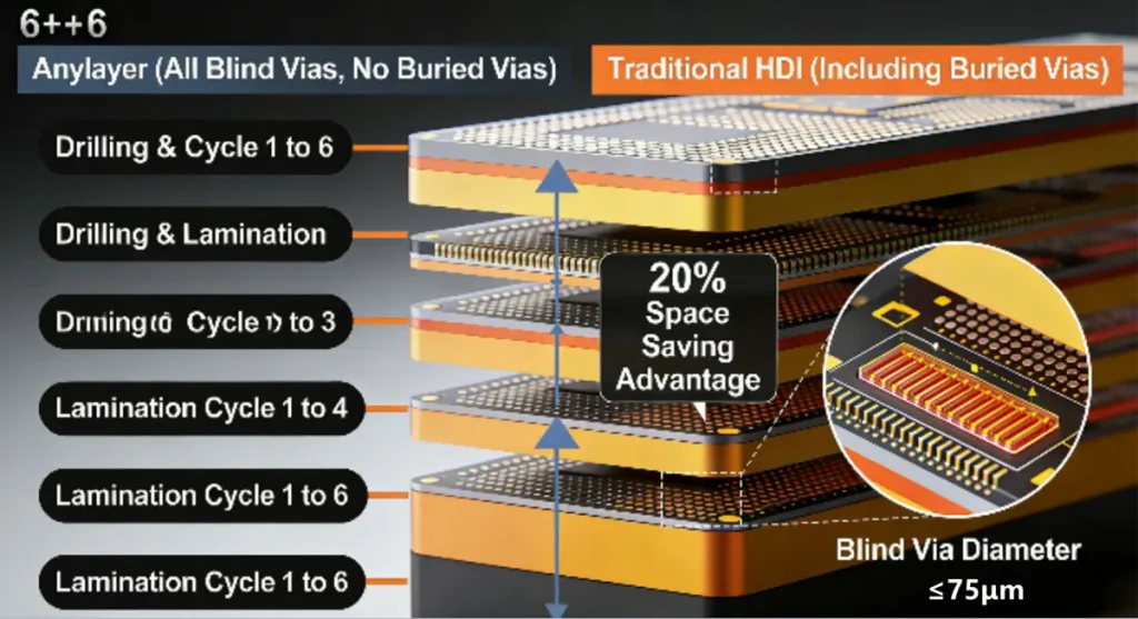
2. Structural Design: From 6+N+6 to Any layer Interconnection
Shenzhen Hongda Circuit Technology Co., Ltd. utilizes a high-precision symmetrical structure design, with mainstream 2026 specifications upgraded to 1+N+1, 2+N+2, 4+N+4, and the latest 6+N+6 multi-order structures.
- 6+N+6 High-Order Structure: This latest 2026 mainstream high-end architecture involves 6 cycles of laser drilling and high-precision lamination. With micro-via diameters ≤75μm, it is optimized for AI servers and 6G R&D.
- Any layer HDI (Arbitrary Layer Interconnection): As a core choice for the 2026 ultra-high-end market, this design abandons traditional buried vias in favor of ultra-fine laser blind vias. This allows free interconnection between any layers, significantly improving integration density and signal efficiency for quantum computing and aerospace electronics.
- Order Definition: The order of an HDI PCB is defined by the number of laser blind via manufacturing and lamination processes, with each stage requiring an independent high-precision lamination cycle.
3. Core Hole Filling and Material Technology for 2026
To meet the requirements of PCIe 6.0 and other high-speed protocols, Shenzhen Hongda Circuit Technology Co., Ltd. has established a sophisticated process matrix:
- High-Precision Electroplating Fill: Utilizing 2026-generation three-in-one horizontal equipment, we achieve high-density direct filling. Plating uniformity error is controlled within 5%, ensuring void-free vias with excellent thermal conductivity and mechanical strength.
- Customized Resin Plugging: For consumer electronics requiring extreme surface flatness, we offer low-dielectric loss epoxy resin filling followed by high-precision copper plating to ensure a dent-free finish.
- Elite Material Formulations: Our 2026 process utilizes M9-grade ultra-low loss copper clad laminates (Dk<3.0, Df<0.005) paired with HVLP5 ultra-thin copper foil and Q-cloth to minimize signal attenuation.
- Precision Control: Internal copper thickness is strictly controlled at 17.1μm, while interlayer alignment precision is maintained within ±10μm.
4. 2026 Manufacturing Capacity Overview
Shenzhen Hongda Circuit Technology Co., Ltd. has fully upgraded its technical indicators to meet diversified market demands, ranging from consumer devices to AI clusters.
| Indicator | Mass Production Standard | Sample Customization Standard |
|---|---|---|
| Layer Count | 4-28 Layers (6+N+6 Mass Production) | 4-78 Layers (Supports 7-order HDI) |
| Min. Trace Width/Spacing | 1.8mil / 1.8mil (0.045mm) | 1.0mil / 1.0mil (0.025mm) |
| Micro-via Diameter | Blind via 0.05mm / Buried via 0.15mm | Blind via 0.02mm / Buried via 0.08mm |
| Core Material | M9-grade ultra-low loss CCL | M9-grade / Isola185HR+RO4000 Mixed |
| Advanced Processes | mSAP & Ultra-fast Laser Drilling | Co WoS / Chiplet Packaging Compatible |
5. Industry Applications: Powering 2026 Benchmark Projects
Shenzhen Hongda Circuit Technology Co., Ltd. HDI products are deeply integrated into the core of the global high-end industrial chain:
- AI Computing: Supporting the NVIDIA Rubin architecture, our 6+N+6 and Any layer boards handle 224Gbps ultra-high-speed signals. The single-machine value for these AI server boards reaches $8,000–$12,000.
- Automotive Electronics: Tailored for 800V high-voltage platforms and L4 autonomous driving, our products utilize thick copper (2-6oz) and high-voltage resistant materials to ensure thermal stability.
- High-Speed Communication: Powering 1.6T optical modules and switches, our solutions maintain ultra-low signal attenuation (Df≤0.003) to solve high-speed transmission loss.
- Cutting-Edge Technology: Utilizing 7-order HDI and Any layer technology, we provide high-reliability components for quantum computing and high-precision medical devices.