High Frequency PCB Manufacturing Capability 2026 | Shenzhen Hongda Circuit Technology
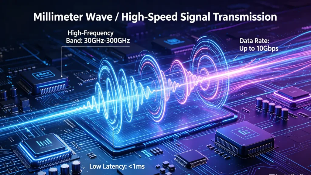
High frequency PCBs remain the core foundation for 5G/6G communication, radar, aerospace, and high-speed AI servers in 2026. As signal frequencies move toward 28 GHz, 56 GHz, and even terahertz bands, and data rates exceed 112 Gbps / 224 Gbps, conventional FR-4 can no longer meet strict low-loss, stable dielectric constant, and high-precision requirements. The rapid evolution of next-generation technologies—including 6G test networks, advanced aerospace avionics, and AI Chiplet integration—has raised the bar for high frequency PCB performance, demanding tighter tolerances, lower signal attenuation, and higher reliability. Shenzhen Hongda Circuit Technology Co., Ltd., a professional manufacturer with years of experience in PCB production, upgrades its high frequency PCB manufacturing capability in 2026 to support these cutting-edge high-speed and millimeter-wave products, providing global customers with tailored, high-performance solutions.
1. Advanced Low-DK & Low-DF Material System (2026 Standard)
Material is the first barrier for high frequency performance, as dielectric constant (Dk) and dissipation factor (Df) directly determine signal loss and stability at high frequencies. In 2026, Hongda Circuit has optimized its material supply chain and now mass-produces high frequency boards with M9-grade, PTFE (Polytetrafluoroethylene), and hydrocarbon laminates—three types of materials that cover different application scenarios and cost requirements. Our material specifications meet 2026 industry standards, with Dk ranging from 2.2 to 3.5 @ 10 GHz (stable within ±0.05, ensuring consistent signal transmission), Df as low as 0.0005 to 0.002 @ 10 GHz (minimizing energy loss), high glass transition temperature (Tg ≥200°C) for resistance to high temperatures in harsh environments, anti-CAF (Conductive Anodic Filament) properties to prevent short circuits, and excellent thermal stability for long-term use.
We cooperate with world-renowned material brands, including Rogers (RO4000/RO3000 series), Isola, and Panasonic Megtron, as well as high-quality domestic high-frequency laminates, ensuring material quality and supply stability. In 2026, we fully support hybrid stacking technology—combining FR-4 with low-loss materials—to balance performance and cost, a solution widely used in 5G base station antennas, RF modules, and high-speed backplanes. This hybrid design reduces overall costs while ensuring that key signal layers maintain low-loss performance, making it an ideal choice for mid-to-high-end consumer electronics and industrial equipment.
2. Ultra-Low-Roughness Copper Foil & Low-Loss Fabrication
At high frequencies (above 10 GHz), the skin effect dominates conductor loss—signal current tends to flow along the surface of the copper foil, so the roughness of the copper foil surface directly affects signal attenuation. To address this, Hongda Circuit adopts mirror-grade ultra-low-profile (ULP/HVLP) copper foil with Ra ≤0.15 μm in 2026, which reduces conductor loss by 25–30% @ 28–56 GHz compared to conventional copper foil. This improvement significantly enhances insertion loss and eye-diagram performance for 56 GHz millimeter-wave circuits, ensuring clear and stable signal transmission in high-speed applications.
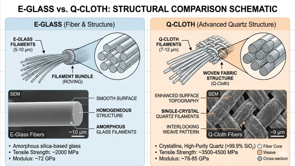
In addition, we replace traditional E-glass cloth with quartz glass cloth (Q-cloth) in the fabrication process. Q-cloth has a lower Dk value and better dimensional stability, which further reduces dielectric loss and improves the high-frequency stability of PCBs. Our fabrication process also includes strict surface treatment—such as chemical cleaning and micro-etching—to ensure good adhesion between copper foil and substrate, preventing delamination and improving the reliability of high frequency PCBs in extreme environments.
3. High Precision Impedance Control & Tolerance
Impedance consistency is critical for RF signal integrity, as impedance mismatches can cause signal reflection, attenuation, and interference. In 2026, Hongda Circuit has upgraded its impedance control capabilities to meet the strict requirements of next-generation high-frequency products. Our standard impedance tolerance for single-ended impedance is 50 Ω ±3% / ±2 Ω, and for differential impedance is 100 Ω ±5% / ±4 Ω—far exceeding industry average standards. We also achieve precise control of line width/space, with a minimum of 20 μm and a standard of 25 μm / 25 μm, and dielectric thickness tolerance of ±0.02 mm.
To ensure impedance consistency from design to manufacturing, we implement IPC-2221 standards and electromagnetic simulation before production. Our engineering team uses professional simulation software to optimize PCB layout, predict impedance values, and adjust design parameters in advance, avoiding production defects caused by impedance mismatches. Additionally, we conduct 100% impedance testing for each high-frequency PCB, using advanced testing equipment to ensure that every product meets the required tolerance standards.
4. Advanced Drilling & Laser Microvia Technology
High frequency PCBs require smooth hole walls and minimal stub resonance, as rough hole walls can cause signal reflection and attenuation, while stub resonance affects signal integrity at high speeds. Hongda Circuit has upgraded its drilling and laser microvia technology in 2026 to address these challenges. Our laser microvias have a diameter of 0.1 mm ±0.02 mm and position accuracy of ±25 μm, ensuring precise connection between layers. For mechanical drilling, we achieve an aspect ratio of ≤12:1 and hole wall copper thickness of ≥25 μm, ensuring good conductivity and reliability.
Back-drilling is now standard for ≥10 Gbps high-speed boards, which eliminates via stub resonance by removing the unused part of the via, reducing signal reflection and improving signal integrity. Our back-drilling process is highly precise, with a depth tolerance of ±0.05 mm, ensuring that the stub length is controlled within the optimal range for high-frequency signals.
5. AI-Driven Process & Quality Control & Typical Applications
To improve production efficiency and product quality, Hongda Circuit applies AI intelligent manufacturing in 2026. Our AI-assisted electromagnetic simulation shortens the R&D cycle by 30%, allowing us to quickly respond to customer design needs and optimize PCB performance. We also use automated optical inspection (AOI) + AI defect recognition, which improves yield by 15% compared to traditional inspection methods, as AI can quickly identify subtle defects such as line scratches, copper residues, and impedance anomalies that are difficult to detect manually. For all high-frequency orders, we conduct 100% impedance and insertion loss testing, ensuring that each product meets the highest quality standards.
Our 2026 high frequency PCBs are widely used in key fields: 5G/6G (millimeter-wave antennas, RF transceivers, power amplifiers), aerospace & defense (radar, satellite communication, avionics), high-speed AI servers (112 Gbps / 224 Gbps backplanes, Chiplet carriers), and automotive radar (24 GHz / 77 GHz / 94 GHz ADAS radar PCBs). We have established long-term cooperation with customers in these fields, providing reliable high frequency PCB solutions that support their technological innovation.
Conclusion In 2026, Shenzhen Hongda Circuit Technology Co., Ltd. continues to deepen high frequency PCB technology, upgrading materials, precision, and intelligent manufacturing capabilities to keep pace with the rapid development of 5G/6G, aerospace, and high-speed AI infrastructure. We are committed to providing low loss, high stability, and high reliability high frequency PCB solutions for global customers, with a focus on quality, innovation, and customer satisfaction. Our professional engineering team, advanced production equipment, and strict quality control system
FAQ
Q1: What is a high frequency PCB?
A: A PCB designed for ≥1 GHz signals, requiring low Dk, low Df, tight impedance control, and low loss. Typical applications: 5G RF, radar, and high‑speed communication.
Q2: When should I choose high‑frequency material instead of FR‑4?
A: When frequency >2 GHz or data rate >10 Gbps, FR‑4 loss becomes unacceptable. 25 Gbps+ almost always requires low‑loss laminates.
Q3: What Dk/Df values do you offer for 2026?
A: Dk 2.2–3.5 @ 10 GHz, Df 0.0005–0.002 @ 10 GHz, with M9, PTFE, and hydrocarbon materials available.
Q4: What impedance tolerance can you achieve?
A: Standard ±5%; high precision ±2–3% for 50 Ω single‑ended and 100 Ω differential.
Q5: Do you offer back‑drilling for high‑speed designs?
A: Yes, back‑drilling is standard for ≥10 Gbps boards to reduce via stub resonance.
Q6: What is your maximum layer count for high frequency PCBs?
A: Up to 78 layers for high‑speed backplanes; 4–24 layers for RF/millimeter‑wave boards.
Q7: Can you support hybrid FR‑4 + low‑loss material stacking?
A: Yes, hybrid stacking is available to balance performance and cost for 5G and high‑speed modules.
Still, need help? Contact Us: sales@pcbkr.com
Need a PCB or PCBA quote? Quote now