These advanced devices are indeed the core guarantee for manufacturing high-standard AI Server PCBs, EV hardware and IC substrates. Aligned with our business positioning, this full set of equipment fully covers all key links from precision processing to high-frequency testing.
Below is a detailed analysis of how these facilities underpin our manufacturing capabilities in the fields of AI servers, 800V electric drive systems and 6G equipment:
Core Manufacturing & Process Capabilities
Precision Pattern Transfer
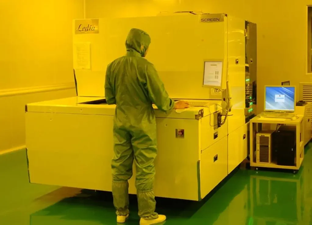
With the SCREEN Ledia LDI Exposure Machine, we achieve ultra-high-precision circuit exposure. LDI (Laser Direct Imaging) technology is indispensable for producing High-Density Interconnect (HDI) boards and IC substrates, enabling consistent ultra-fine line width and spacing even in complex multilayer PCB designs.
High Aspect Ratio Microvia Machining
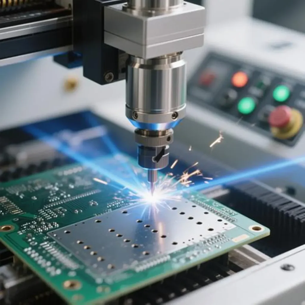
The Mitsubishi Electric UV/CO₂ Laser Drilling Machine for PCB & IC Substrate is dedicated to blind and buried hole drilling. UV/CO₂ hybrid laser technology is critical for microvia fabrication in mSAP processes commonly used in AI server products, as well as high-layer-count boards such as 104-layer backplanes.
High-Performance Lamination
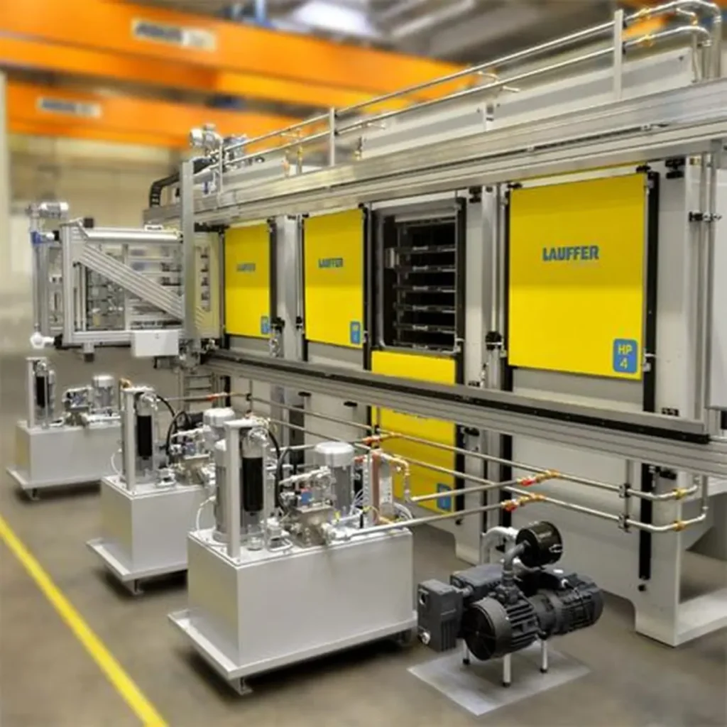
The Lauffer PCB Lamination System is a well-recognized high-end lamination solution in the industry, delivering precise control over temperature and pressure uniformity. It is essential for multilayer boards using low-loss materials like Rogers, Taconic or M9 dielectric substrates, effectively preventing board warpage and ensuring consistent interlayer dielectric thickness.
Automated Electroplating
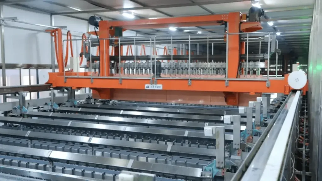
The HX Automation PCB Plating Line delivers continuous and stable surface treatment and via copper plating performance. For high-current thick copper PCBs required by 800V EV power electronic equipment and deep-hole electroplating of high-layer backplanes, the automated plating line ensures superior and consistent quality.
Quality Inspection & Signal Integrity Assurance
High-Frequency Signal Testing
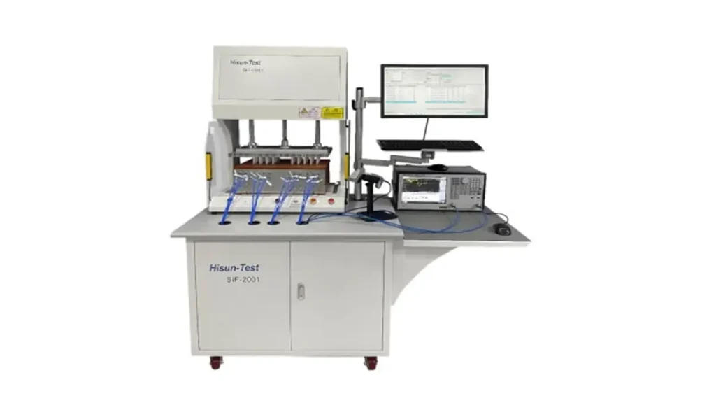
The Hisun-Test SIF-2001 Automatic Impedance Test System (equipped with Keysight VNA) serves as the core solution for 112G/224G PAM4 technology. Paired with the Keysight Vector Network Analyzer (VNA), the system accurately measures differential impedance and insertion loss, guaranteeing signal integrity for AI servers under high-speed transmission conditions.
Non-Destructive Internal Defect Inspection
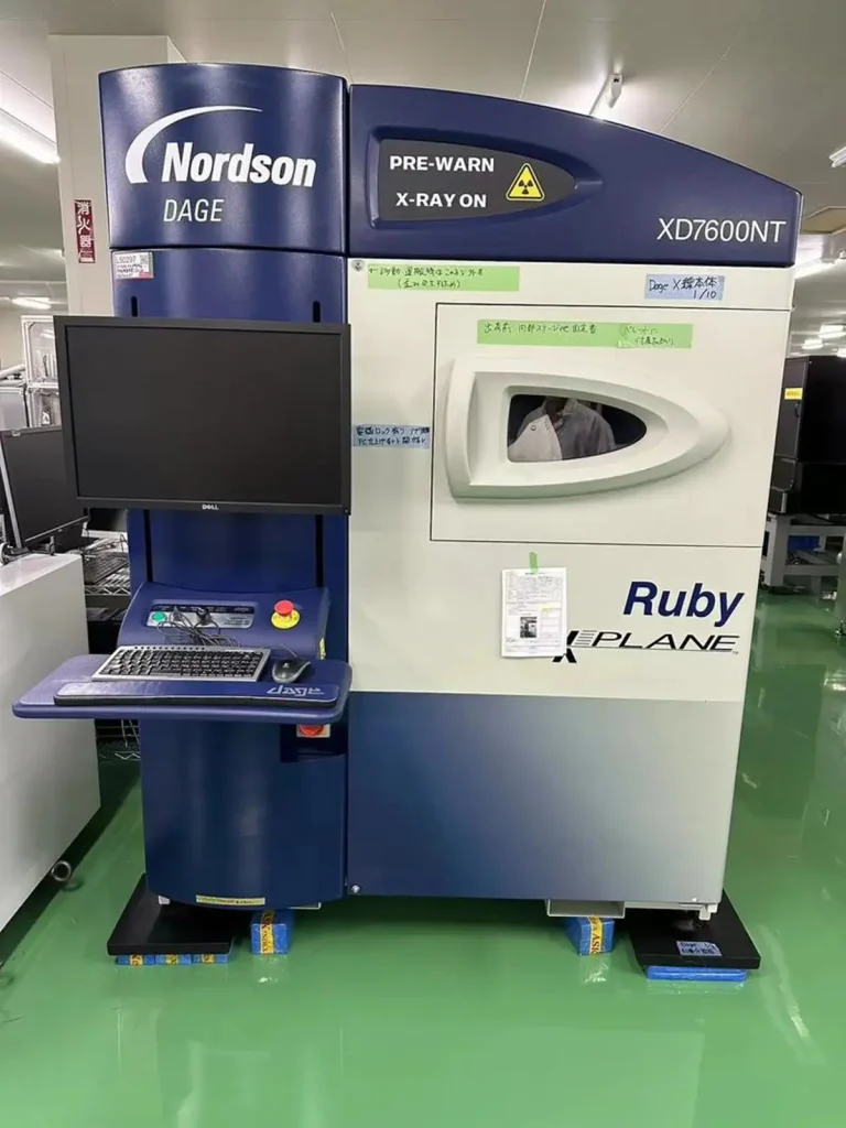
The Nordson DAGE XD7600NT X-Ray Tester inspects BGA soldering quality, via alignment and internal structure of multilayer PCBs. For the production of CoWoS substrates and high-layer-count backplanes, X-Ray inspection is vital for detecting hidden internal defects and maintaining yield at the PPM (Parts Per Million) level.
Summary
Equipped with this complete equipment cluster from top-tier brands including SCREEN, Mitsubishi, Lauffer and Nordson DAGE, Shenzhen Hongda Circuit (PCBKR) has established solid hardware foundations to manufacture the following high-end products:
- AI Server Motherboards: Supporting ultra-high layer counts up to 104 layers and PAM4 high-speed signal transmission.
- IC Substrates & CoWoS Substrates: Meeting micron-level precision processing requirements.
- 800V EV & 6G Devices: Delivering high-reliability processing solutions for low-loss specialty materials.
This full suite of equipment not only optimizes our TTM (Time to Market) efficiency, but also provides strong production backing for our No MOQ policy and round-the-clock 24/7 DFM technical support.