PCB Manufacturing Services for AI Server OEMs
Shenzhen Hongda Circuit Technology Co., Ltd. provides PCB manufacturing services for AI server OEMs that require 24+ layer high-speed boards, HDI interconnects, tight impedance control, low-loss materials, and scalable delivery. The key challenge is not simply fabricating a board—it is achieving signal integrity, thermal stability, and supply continuity at production volumes.
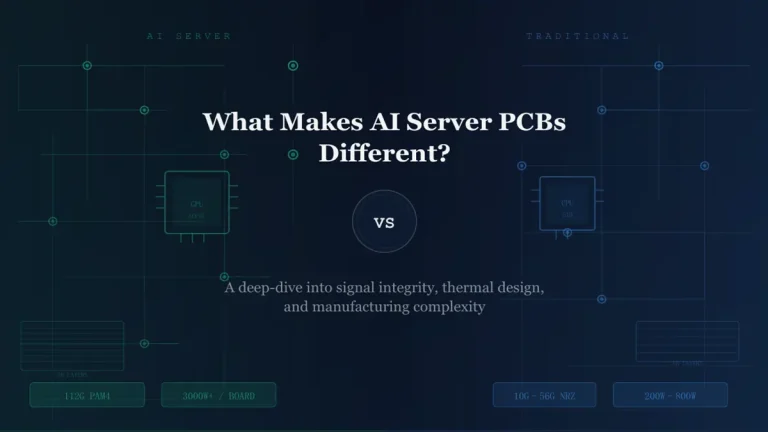
Why are AI server OEMs demanding 24+ layer, low-loss PCB manufacturing?
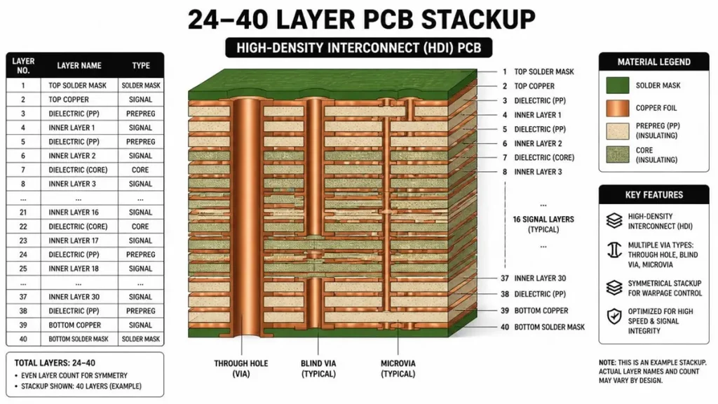
24-40 Layer AI Server PCB Stackup Diagram – Shenzhen Hongda Circuit
Modern AI servers routinely integrate high-speed PCIe, Ethernet, and accelerator interconnects that require 24–40 layer PCB stackups, HDI structures, and low-Dk/Df laminates to maintain signal integrity and reduce insertion loss at high data rates.
Typical technical requirements for AI server boards
| Parameter | Typical Requirement |
| Layer count | 24–40 layers |
| Board thickness | 3.2–6.4 mm |
| Impedance tolerance | ±5% or tighter |
| Line/space | 50/50 µm to 75/75 µm |
| Via technology | Laser microvia, stacked or staggered HDI |
| Surface finish | ENIG, EPIG, immersion silver, or selective gold |
| Materials | Low-loss hydrocarbon, PTFE hybrid, or high-speed epoxy systems |
turnkey PCB for AI servers detailed manufacturing pain points
- Insertion loss accumulationA 32-layer backplane can contain more than 10 signal layer transitions. Each via stub and copper roughness variation increases loss and reflection.
- Registration drift during sequential laminationLarge AI motherboards and backplanes often exceed 450 mm in one dimension. Multiple lamination cycles can create cumulative X/Y dimensional changes.
- Warp and twist under heavy copper loadingPower delivery networks for GPU accelerators commonly use 2–4 oz copper in selected layers, creating asymmetrical stress during lamination and reflow.
- Thermal hotspots around VRMs and accelerator connectorsLocalized heat density can exceed several hundred watts per board region, requiring copper balancing, thermal via arrays, and heat-spreading strategies.
Scenario example
An AI accelerator carrier board with multiple high-current GPU connectors requires both ultra-low-loss differential pairs and thick copper power planes. In practice, balancing signal performance and thermal management is often the dominant engineering challenge rather than drilling or imaging capability alone.
How does NPI support and DFM/DFA review reduce AI server launch risk?
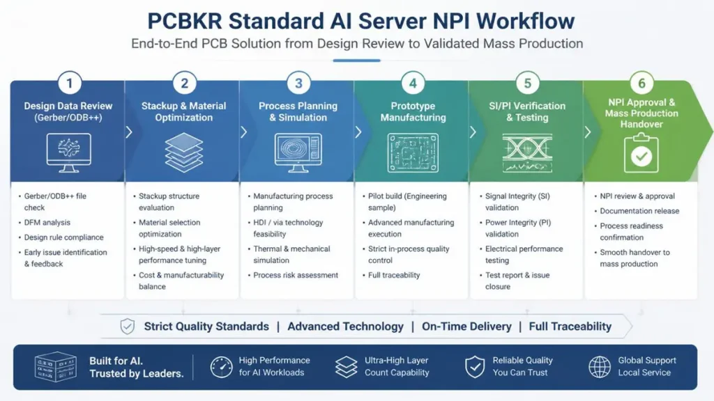
PCBKR Standard AI Server NPI Workflow Chart
NPI support identifies manufacturability and assembly risks before tooling and production, reducing costly redesigns, schedule slips, and yield loss during ramp-up.
A typical AI server NPI workflow
- Gerber, ODB++, and netlist review
- Stackup optimization for target impedance and loss budget
- Via structure selection (stacked vs. staggered microvia)
- Backdrill feasibility analysis
- SMT land pattern and BGA escape routing review
- Prototype fabrication and SI/PI validation support
turnkey PCB for AI servers detailed manufacturing pain points
- BGA escape congestionA 0.8 mm or finer pitch BGA can force aggressive HDI routing that exceeds practical fabrication capability if not reviewed early.
- Backdrill over-penetrationIf drill tolerances and stackup shrinkage are not modeled, excessive backdrill depth can damage target layers.
- Impedance mismatch across connector transitionsAI server architectures often combine mezzanine connectors, backplanes, and daughter cards; transition discontinuities can dominate the channel budget.
- Assembly shadowingTall heatsinks and connectors can block AOI visibility and complicate rework planning.
Original engineering insight
One recurring issue in AI server projects is that the electrical model assumes ideal via structures, while the manufacturing reality includes copper plating variation, resin recession, and drill wander. Experienced DFM teams model these effects before prototype release instead of after the first signal-integrity failure.
How do quality traceability and stable supply impact AI server OEMs?
For AI server OEMs, quality traceability is critical because field failures are expensive and difficult to isolate. Stable supply is equally important because production schedules are often constrained by accelerator and networking component availability.
Recommended quality controls
| Control Area | Purpose |
| MES traceability | Track material lots, process parameters, and inspection records |
| SPC monitoring | Control plating thickness, etch compensation, and impedance variation |
| FMEA review | Identify high-risk failure modes before production |
| X-Ray inspection | Verify BGA solder joints and buried features |
| Cross-section analysis | Validate microvia fill, copper thickness, and layer alignment |
| Thermal stress testing | Screen for delamination, CAF risk, and via reliability |
turnkey PCB for AI servers detailed manufacturing pain points
- Lot-to-lot impedance driftChanging laminate lots can shift dielectric properties and affect high-speed channels.
- Microvia reliability in sequential laminationStacked microvias can crack under thermal cycling if copper filling and resin support are not optimized.
- Component shortage substitutionsAlternate parts may change footprint, thermal behavior, or signal characteristics, requiring engineering revalidation.
- Global delivery variabilityTransit disruptions can affect ramp schedules unless buffer inventory and multi-region logistics are planned.
Scenario example
A cloud infrastructure customer may qualify a server platform for 3–5 years of deployment. In that context, traceability is not just a quality requirement; it is a lifecycle management requirement. When a field issue appears, the OEM must quickly identify affected material lots and production batches.
What OEM cooperation model works best for AI server programs?
The optimal model depends on design maturity. Mature designs often use consignment manufacturing, while new AI platforms benefit from co-development and turnkey manufacturing support.
Common cooperation models
| Model | Best For |
| Consignment | OEM provides BOM and design; supplier focuses on fabrication and assembly |
| Co-development | New platforms requiring SI/PI optimization and manufacturability tuning |
| Custom turnkey | End-to-end delivery from PCB fabrication through PCBA and testing |
turnkey PCB for AI servers detailed manufacturing pain points
- Specification ownership gapsWithout clear ownership, stackup changes and impedance targets can become ambiguous.
- Revision synchronizationAI hardware programs often iterate rapidly; mismatched PCB revisions can create expensive assembly scrap.
- Thermal-mechanical co-design challengesBoard stiffness, heatsink loading, and connector retention must be coordinated across mechanical and electrical teams.
Original engineering insight
In co-development projects, the most effective reviews combine SI engineers, PCB process engineers, and SMT engineers in the same session. Many high-speed problems that appear electrical are actually manufacturing-induced discontinuities that become visible only when all three disciplines review the design together.
What value-added services matter most for AI server OEMs?
Beyond bare PCB fabrication, AI server OEMs increasingly require component sourcing, advanced assembly, comprehensive testing, and accelerated prototype services to shorten time-to-market.
High-value services for AI server programs
| Service | Benefit |
| BOM management | Mitigates component shortages and lead-time risk |
| Advanced SMT | Supports large BGAs, fine-pitch devices, and high-density connectors |
| AOI + X-Ray + ICT + FCT | Improves detection coverage from solder defects to functional issues |
| Thermal potting/encapsulation | Enhances environmental and thermal robustness |
| Fast-turn prototyping | Accelerates SI/PI model validation and design iteration |
turnkey PCB for AI servers detailed manufacturing pain points
- Large BGA void controlHigh-power accelerator packages can be sensitive to solder voiding and thermal resistance.
- Connector coplanarityDense high-speed connectors require tight placement and solder planarity control.
- Thermal interface reliabilityPotting compounds and thermal fillers must be compatible with rework and long-term aging requirements.
- Prototype-to-production transferA prototype that works electrically may still fail yield targets if panel utilization, drill density, and assembly throughput are not considered early.
Scenario example
During an AI server bring-up, engineering teams often need multiple PCB revisions in quick succession. Fast-turn prototype capability is valuable only if the supplier can also maintain the same stackup, material set, and impedance process that will be used in production. Otherwise, SI correlation between prototype and production becomes unreliable.
For AI server OEMs, selecting a PCB manufacturing partner is fundamentally a risk-management decision. The critical capabilities are high-layer fabrication, HDI expertise, tight impedance control, low-loss material processing, NPI collaboration, traceability, and supply stability. Shenzhen Hongda Circuit Technology Co., Ltd. positions its PCB manufacturing services around these requirements to support AI server, accelerator, and high-performance computing programs from prototype through volume production.
FAQ: PCB Manufacturing Services for AI Server OEMs
What is the practical difference between a standard server PCB and an AI server PCB?
A standard server PCB may operate with lower channel bandwidth and simpler stackups. AI server PCBs typically require 24+ layers, HDI routing, tighter impedance control, and lower-loss materials to support high-speed accelerator interconnects and dense power delivery.
How does HDI compare with traditional through-hole routing for AI servers?
HDI reduces routing congestion and shortens signal paths through laser microvias and finer features. Traditional through-hole routing is generally less expensive but consumes more routing area and can introduce longer via stubs that degrade high-speed performance.
Why are low-loss materials preferred over standard FR-4 in AI server designs?
Low-loss laminates exhibit lower dielectric loss (Df), reducing insertion loss and improving signal integrity over long channels. Standard FR-4 may be adequate for lower-speed applications, but AI server channels often benefit from materials specifically optimized for high-frequency performance.
What is the difference between prototype PCB service and production PCB service for AI hardware?
Prototype service prioritizes speed and engineering flexibility, while production service prioritizes yield, repeatability, traceability, and supply continuity. For AI hardware, maintaining stackup and process consistency between prototype and production is especially important for SI correlation.
How does turnkey AI server PCB manufacturing compare with consignment manufacturing?
In turnkey manufacturing, the supplier manages PCB fabrication, component sourcing, assembly, testing, and logistics. In consignment manufacturing, the OEM supplies the BOM and often the components, while the supplier focuses on fabrication and assembly execution. Turnkey can simplify coordination; consignment can provide tighter OEM control over strategic components.
Find Out About Us: Delivering Top-Tier Fabrication for Both AI & Conventional PCBs
Navigating the line between cutting-edge innovation and high-volume, cost-effective production shouldn’t be a compromise. At Shenzhen Hongda Circuit Technology (PCBKR), we bridge this gap by elevating the manufacturing standards for both high-performance AI hardware and traditional multi-layer PCBs.
By integrating advanced manufacturing methodologies across all production lines, we bring an elite level of precision to traditional PCB fabrication. Our standard boards benefit from enhanced interlayer alignment tolerances (down from ±75μm to within ±25μm) and tightened differential impedance control (±5%). Supported by 100% 3D X-Ray (AXI) inspection, your conventional boards achieve chip-level reliability, superb signal stability, and near-100% yield.
Your Strategic Manufacturing Partner
We proudly stand as a dual-capability partner: offering the elite technical ceiling required for next-gen AI hardware, while maintaining the exceptional flexibility, rapid turnaround, and unmatched cost-efficiency needed for mid-to-high-volume traditional board campaigns. You get zero-defect reliability without the premium overhead or bureaucracy of massive tier-1 factories.
Ready to upgrade your hardware’s reliability?
Submit your Gerber files today for an agile engineering review and a highly competitive quote.
📧 Contact our experts: sales@pcbkr.com
About Author
David Chen https://www.linkedin.com/in/pcbcoming
David Chen boasts an extensive professional background in PCBA manufacturing, PCBA testing, and PCBA optimization, with specialized expertise in high-precision PCBA fault analysis and rigorous PCBA reliability testing. The author has worked with high-layer-count server PCB fabrication, ultra-low-loss backplane stackups, and thermo-mechanical reliability optimization for AI infrastructure projects involving 112G and 224G PAM4 architectures. Skilled in complex circuit design and cutting-edge advanced PCB manufacturing processes, he delivers solutions that elevate product durability and performance across industrial applications. His technical articles focusing on PCBA manufacturing workflows and testing methodologies are widely cited by industry peers, research institutions, and technical platforms, solidifying his reputation as a recognized technical authority in the global circuit board manufacturing sector.