Standard Process
Material: KB6061, S1141, S1000, IT180
Layer: 4-120 Layer
Solder Mask Color: Green/White/Blue/Red
Silk Screen Color: White/Black
Thickness: 0.3-6.0mm
Copper Thickness: 0.5-6OZ
Surface Treatment: Immersion Gold/OSP/HASL
Min Trace/Space: 3mil(0.075mm)
Min Hole Size: 0.15mm
Aspect Ratio: ≤8:1 (Std), ≤12:1 (HDI)
Impedance Control: ±5%
Testing: AOI, Flying Probe, Thermal Stress
Application: Consumer electronics
Product Details
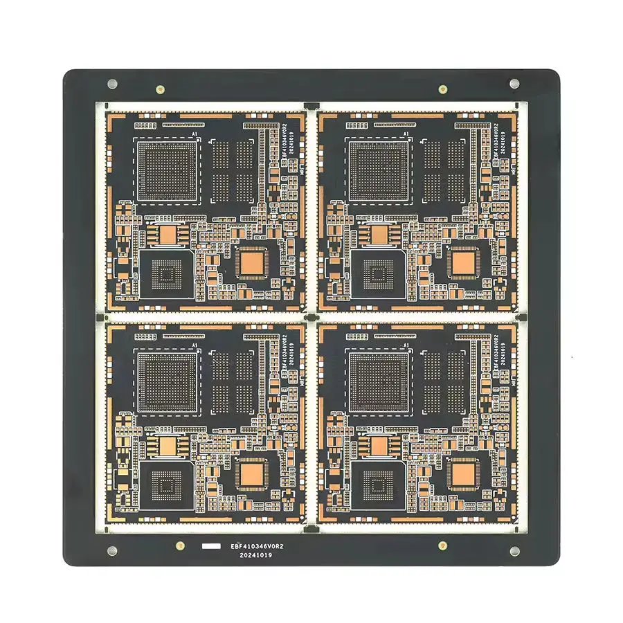
What is a Multilayer PCB?
A Multilayer Printed Circuit Board (PCB) integrates three or more conductive copper layers bonded with dielectric prepreg and core materials, interconnected by through vias, blind vias, buried vias, or microvias. Unlike single‑ or double‑sided PCBs, multilayer boards integrate internal power, ground, and high‑speed signal layers, enabling higher density, better EMC performance, and stronger thermal management—critical for 2026 high‑speed electronics.
At Shenzhen Hongda Circuit Technology Co., Ltd., we focus on even‑layer stackup designs (4L, 6L, 8L, up to 64L) with precision lamination and interlayer alignment, delivering stable electrical performance and long‑term reliability.
Why Multilayer PCBs Lead 2026 Electronics Innovation
Driven by AI computing, 5G/6G, advanced packaging, and miniaturization, multilayer PCBs have become the core of high‑end electronic systems. Key trends in 2026:
- Ultra‑High Density: HDI Any‑layer, finer lines, smaller vias, higher component density
- High‑Speed & Low Loss: Low‑Df materials for 224Gbps+ transmission with minimal signal attenuation
- Ultra‑Thin & High‑Layer: Thin‑core multilayers and high‑layer boards for servers and optical modules
- Rigid‑Flex Integration: Multilayer flex and rigid‑flex for wearable, folding, and automotive scenarios
- Smart Manufacturing: AI‑aided inspection, automatic impedance control, and digital traceability
2026 Advanced Manufacturing Process (Hongda Exclusive)
Our fully upgraded process ensures precision, stability, and consistency for high‑end multilayer PCBs:
- Material Cutting → 2. Inner Layer Imaging (LDI) → 3. AOI Inspection → 4. Black Oxide / Plasma Treatment
- Precision Lamination (PinLAM / Rivet / Fusion Bonding) → 6. CNC Drilling / Laser Drilling
- Desmear & Electroless Copper → 8. Pattern Plating → 9. Etching & AOI
- Solder Mask & Legend Printing → 11. Surface Finish → 12. Depth Routing / V‑Cut
- Back Drilling (Optional) → 14. Impedance Test / E‑Test → 15. Vacuum Packaging
Core Advantages of Hongda Multilayer PCB (2026)
- 2026 Cutting‑Edge Technologies: Any‑layer HDI, Back Drilling, mSAP, Low‑Loss M9 Materials
- Ultra‑High Precision: Min. 2mil lines/spaces, laser microvias, tight impedance control
- AI‑Smart Factory: Full automation, AI AOI, real‑time quality monitoring
- High‑Layer Stability: 4–120L mass production for AI servers and communication equipment
- Rigid‑Flex Expertise: Multilayer flex & rigid‑flex for high‑reliability applications
- Full Compliance: IPC‑A‑600, IPC‑4101, RoHS, REACH, automotive‑grade reliability
Difference Between Single/Double‑Sided & Multilayer PCBs
The key difference is the integration of internal power/ground layers and dedicated high‑speed routing layers. Multilayer PCBs:
- Improve signal integrity and EMC performance
- Support higher component density and miniaturization
- Enhance power distribution and thermal management
- Enable complex functions in limited space
Applications
- AI Servers & Data Centers
- 5G/6G Base Stations & Optical Modules
- Automotive ADAS, Infotainment, Power Control
- Medical Imaging & Wearable Devices
- Industrial Control & IoT Gateways
- High-End Consumer Electronics