Standard Process
Outer Copper: 3oz – 50oz (Extreme)
Inner Copper: 3oz – 20oz (Extreme)
Layer Count: Up to 28 Layers (Hybrid Stack-up)
Board Thickness: 0.8mm – 10.0mm
Tolerance: ±5% (Precision Pulse Plating)
3oz: 0.20mm / 0.20mm (8/8 mil)
6oz: 0.40mm / 0.45mm (16/18 mil)
10oz: 0.65mm / 0.75mm (26/30 mil)
20oz+: 1.0mm+ / 1.2mm+
Aspect Ratio: 15:1 (Advanced)
Via Filling: Vacuum Epoxy Resin + Copper Capping (IPC-4761 Type VII)
Min. Drill: 0.3mm (scales with copper weight)
Substrate: High-Tg FR-4 (170°C–180°C), Ceramic-filled Hydrocarbon (Rogers), Metal Clad.
Thermal Conductivity: Specialized prepregs > 1.5 W/mK.
Surface Finish: ENIG, ENEPIG, Immersion Tin (for Press-fit).
mSAP for Heavy Copper: Precision vertical sidewall traces for 3oz–5oz.
Embedded Busbars: Integrated solid copper for 500A+ currents.
LDI Solder Mask: Laser Direct Imaging for high-topography trace coverage.
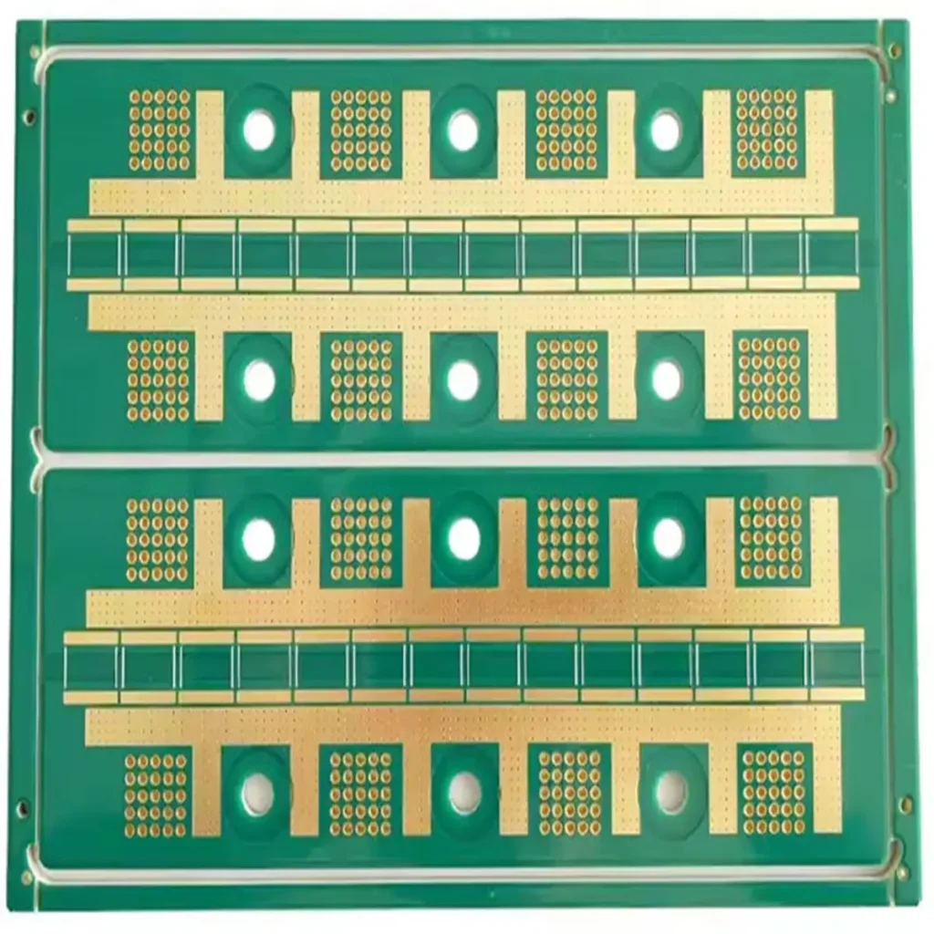
Product Details
The 2026 Definitive Guide to Heavy Copper PCB Manufacturing: High-Power Solutions for the AI and EV Era
By: Shenzhen Hongda Circuit Technology Co., Ltd.
Introduction
As we move through 2026, the global demand for high-performance power electronics has reached an unprecedented peak. Driven by the massive power requirements of AI Data Centers (GPU clusters) and the transition to 800V Electric Vehicle (EV) architectures, the Heavy Copper PCB has evolved from a niche component into a critical thermal and electrical management solution.
At Shenzhen Hongda Circuit Technology Co., Ltd., we have integrated next-generation fabrication processes to push the boundaries of what thick copper circuits can achieve.
1. Redefining “Heavy” and “Extreme” Copper
While the industry historically defined “Heavy Copper” as anything over 3oz, 2026 standards have shifted to accommodate extreme power densities.
- Standard Heavy Copper: 3oz – 10oz (Ideal for industrial power supplies and automotive converters).
- Extreme Copper (Ultra-Thick): 11oz – 50oz (Essential for AI server power rails, grid-scale energy storage, and heavy-duty military hardware).
Hongda Circuit Advantage: We offer a seamless transition from 3oz prototyping to 50oz mass production, ensuring vertical integration for your most demanding projects.
2. 2026 Advanced Manufacturing Capabilities
Modern power electronics require more than just thick copper; they require precision. Our 2026 technical parameters set a new benchmark:
| Feature | Advanced 2026 Specification (Hongda) | Industry Benchmark (2024-2025) |
| Max Finished Copper (Outer) | 50oz (1750μm) | 15oz – 20oz |
| Max Finished Copper (Inner) | 20oz (700μm) | 10oz – 12oz |
| Layer Count (Hybrid Weight) | Up to 28 Layers | 12 – 20 Layers |
| Max Board Thickness | 10.0mm | 6.5mm |
| Copper Thickness Tolerance | ±5% (Precision Plating) | ±10% |
| Thermal Conductivity | >1.5 W/mK (Specialized Prepregs) | ~0.25 W/mK (Standard FR4) |
3. Breakthrough Technologies in Heavy Copper Fabrication
A. mSAP (Modified Semi-Additive Process) for Power
Traditional chemical etching often leads to an “over-etched” trapezoidal trace profile. In 2026, Hongda utilizes mSAP technology for 3oz–6oz layers. This allows for nearly vertical trace sidewalls, enabling tighter spacing and significantly reducing the footprint of high-current paths on AI server motherboards.
B. Embedded Copper Busbars
For currents exceeding 500A, even 50oz copper may not suffice without excessive board width. We now offer Embedded Busbar Technology, where solid copper bars are integrated directly into the inner layers. This provides superior heat dissipation and current carrying capacity while maintaining a standard PCB form factor.
C. IPC-4761 Type VII Via Management
To manage the extreme heat generated by modern GPUs and power modules, our heavy copper boards utilize Vacuum Epoxy Resin Plugging followed by Copper Capping. This ensures 100% reliable thermal vias that can withstand the thermal expansion (CTE) mismatches inherent in thick copper designs.
4. Critical Design Considerations (DFM)
Designing for heavy copper requires a different mindset. At Shenzhen Hongda Circuit Technology Co., Ltd., our engineers focus on three key DFM pillars:
- The Etch Factor: As copper weight increases, the minimum trace width and spacing must also increase. For a 10oz board, we recommend a minimum spacing of 0.75mm (30 mil) to ensure reliable insulation.
- Solder Mask Topography: Thick traces create “valleys.” We use Laser Direct Imaging (LDI) and multiple-pass curtain coating to ensure the shoulders of 20oz traces are fully protected without air bubbles.
- Material Stability: We exclusively use Ultra-High Tg (180°C+) and Halogen-Free materials to prevent delamination during the high-heat assembly processes required for heavy copper components.
5. Why Choose Shenzhen Hongda Circuit Technology?
In a market where reliability is non-negotiable, Shenzhen Hongda Circuit Technology Co., Ltd. stands out through rigorous quality control and technical innovation.
- Precision Plating: Our automated Vertical Continuous Plating (VCP) lines ensure uniform copper distribution across the entire panel.
- Global Compliance: Fully certified to ISO 9001, IATF 16949 (Automotive), and UL safety standards.
- Rapid Response: Get a technical DFM review within 24 hours and expedited prototyping for critical AI and energy projects.
Conclusion
The future of power electronics is thicker, faster, and hotter. Whether you are building the next generation of AI supercomputers or 800V EV drivetrains, Shenzhen Hongda Circuit Technology Co., Ltd. provides the heavy copper solutions needed to power tomorrow.
Contact our engineering team today for a custom quote or DFM consultation.