IC Substrate Board – 2026 Advanced Manufacturing Capabilities
Technical Excellence & 2026 Next-Gen Technology Leadership
For comprehensive details on Shenzhen Hongda Circuit Technology Co., Ltd.’s industry-leading IC Substrate technical capabilities and 2026 cutting-edge manufacturing processes, download our 2026 Process Capability Datasheet (updated with latest industry standards). Our engineering team is on standby for technical consultations and custom solutions—reach out anytime for your project needs.
For dedicated IC Substrate Board product specifications and application cases, visit our IC Substrate Board Hub. Encounter design challenges? Download our 2026 IC Substrate Design Rules (Compliant with National Embedded Substrate Standards) or consult Shenzhen Hongda Circuit Technology Co., Ltd.’s senior IC substrate engineers directly via email: PCB@pcbkr.com
2026 IC Substrate Product Roadmap & Technology Evolution
Shenzhen Hongda Circuit Technology Co., Ltd.’s product roadmap is engineered for the era of heterogeneous integration, AI computing and advanced packaging, with mass production capabilities for next-gen substrates and R&D breakthroughs in future-oriented technologies. Our 2026 core product portfolio covers:
- Embedded Component Substrates: Full-series passives/actives embedded, film type embedded, discrete IC embedded (compliant with GB national test standards for embedded substrates)
- Advanced Packaging Substrates: Fan-Out, PLP (Panel Level Packaging) mass production, FC (Flip Chip) full-compatibility, ETS/MSAP/SAP full-additive process integration
- High-Density Interconnect Substrates: FCCSP (BOL & Mass Production), FCBGA (AI chip dedicated), Glass Interposer (Array) with EMIB integration, 10-2-10 glass substrate prototype validation
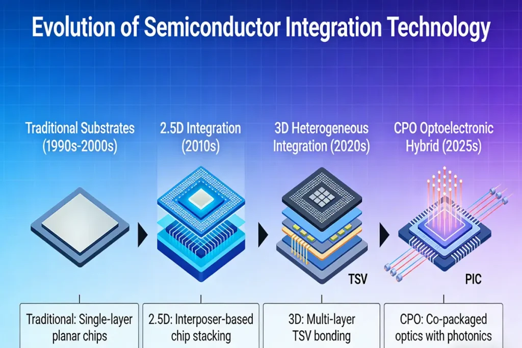
- Specialized Application Substrates: LED PLCC, MEMS, SiP (2.5D/3D heterogeneous integration), EBGA, RF FP, MSD(SD)/eMMC, Busless-CSP, Coreless/Carrier Coreless CSP
- Next-Gen Architecture Substrates: CoWoP (Chip on Wafer on PCB) compatible substrates, CPO (Co-Packaged Optics) photoelectric hybrid substrates, HBM stacking dedicated ABF substrates
2020-2027 Core Technology Roadmap (Unit: μm)
Phase 1: Precision & Density Leap (2020-2025) → Phase 2: 2026-2027 Next-Gen Mass Production (Industry Leading)
| Technical Indicator | 2020 | 2023 | 2025 | 2026 (Mass Production) | 2027 (Flagship) |
|---|---|---|---|---|---|
| Board Thickness/Core/PP | 2L,110/50;4L,220/50/30 | 2L,100/40;4L,170/40/25 | 2L,65 (carrier);4L,150/30/20 | 2L,50 (coreless);8L,200/20/15 | 2L,40 (glass core);12L,250/15/10 |
| Core Process | Tenting | MSAP | ETS/SAP | mSAP/SAP (ultra-fine) | Laser SAP (nano) |
| Line/Space | 35/35 | 30/30 | 25/25 | 8/8 (mass production) | 5/5 (high-end) |
| Finger Pitch | 100 | 80 | 65 | 60 | 50 |
| FC Pad Pitch (Peripheral/Array) | 120/100 | 80/60 | 50/40 | 45/35 | 40/30 |
| BLV/Land | 75/125 | 60/110 | 50/90 | 45/85 | 40/80 |
| Hole/Land (Mech./TCF) | 100/210;75/150 | 75/175;100/150 | 75/160;100/200 | 60/140;100/220 | 50/120;100/250 |
| BGA Pitch | 400 | 350 | 300 | 250 (glass substrate) | 200 (CoWoP) |
2026-2027 Advanced Manufacturing Precision & Material Standards (Unit: μm)
| Category | 2020 | 2023 | 2025 | 2026 (Mass Production) | 2027 (Flagship) |
|---|---|---|---|---|---|
| SM Registration | ±25 | ±15 | ±12.5 | ±10 | ±8 |
| Solder Resist (SRO) | 80 | 70 | 60 | 50 | 40 |
| SM Flatness | ±7 | ±5 | ±3 | ±2 (glass substrate) | ±1.5 (nanoscale) |
| Surface Finish | Ni/Ag/Au;Ni/Au;ENEPIG;OSP | AFOP;Immersion Tin added | SAC305 for SOP | ENEPIG-HD;OSP Ultra-Thin | Optical Coating for CPO |
| Core Materials | HL832NX-A;HL832NS;AMC-832HF | MCL-E-679FGB;DS-7409HGB | HL832NSF;MCL-E-705G | M9 Grade CCL (Quartz fiber);PTFE (low Df) | M10 Grade CCL;Glass Core (3-5ppm/°C CTE) |
| Solder Resist Materials | AUS308;AUS320 | AUS410 | SR-1;SR-2 | SR-3 (low loss);High Thermal Conductivity SR | Photoelectric Hybrid SR (CPO dedicated) |
2026 Flagship IC Substrate Technologies & Product Advantages
System-in-Package Substrate (SiP) – 2026 Heterogeneous Integration Leader
Shenzhen Hongda Circuit Technology Co., Ltd.’s 2026 SiP substrates redefine system-level integration, supporting assembly of multi-source heterogeneous wafers, high-speed sensing components, embedded passives/actives and HBM stacks into a single package. As the ultimate alternative to SoC for high-performance computing, our SiP substrates deliver 15% lower power consumption, 50% higher bandwidth and ultra-compact form factors, accelerating product time-to-market by 30% for AI, automotive and edge computing applications.
Our SiP portfolio covers 2D planar MCM (Multi-chip Module) and 3D stacked packaging (PiP, stacked chip) with ultra-small packaging area, and supports hybrid bonding technologies (Wire Bonding + Flip Chip) for customized signal paths. We pioneer component-embedded multifunctional SiP substrates (compliant with national embedded substrate test standards) and offer fully customizable chip arrangements/bonding solutions for customer-specific product requirements—from consumer electronics to high-end AI servers.
Flip Chip Ball Grid Array Substrate (FCBGA) – 2026 AI Chip Dedicated
Shenzhen Hongda Circuit Technology Co., Ltd.’s 2026 FCBGA substrates are high-density, high-speed semiconductor packaging substrates optimized for LSI chips, microprocessors, GPU/AI accelerators and image processors with ultra-high I/O pin counts. Leveraging mSAP ultra-fine process (8/8μm Line/Space) and M9 grade low-loss materials (Df<0.002), our FCBGA substrates enable 224Gbps PAM4 high-speed transmission and support kilowatt-level chip power supply (25A+ current) with integrated thermal management and PDN (Power Distribution Network) optimization.
For AI server applications, our FCBGA substrates are fully compatible with 5.5x photomask size silicon interposers and support up to 12 HBM4 stacks, delivering unrivaled performance and cost advantages for high-pin-count IC packaging in the AI era.
Flip Chip Chip Scale Package Substrate (FCCSP) – 2026 Cost-Efficient High Density
Shenzhen Hongda Circuit Technology Co., Ltd.’s FCCSP substrates adopt flip-chip bump interconnection (replacing traditional wire bonding) and wafer-level packaging technology, with 2026 mass production capabilities for 45/35μm FC pad pitch and coreless board design. As wafer bump process costs continue to decline, our FCCSP substrates offer an industry-leading cost-performance ratio for high-pin-count ICs, with 30% lower packaging costs and 20% higher reliability compared to conventional solutions.
Our 2026 FCCSP portfolio includes BOL (Beginning of Line) prototypes and mass production for consumer electronics, automotive electronics and industrial control, with full compatibility with panel-level packaging (PLP) for large-scale production efficiency.
Plastic Ball Grid Array Substrate (PBGA) – 2026 Upgraded Cost-Effective Solution
Shenzhen Hongda Circuit Technology Co., Ltd.’s upgraded 2026 PBGA substrates are the foundational ball grid array substrates for wire bonding packaging, using high-modulus glass fiber-impregnated copper foil substrates with improved mechanical stability and thermal conductivity. Ideal for medium-to-high pin count chip packaging, our PBGA substrates address the limitations of traditional lead frame packages in chip function upgrades, offering a highly cost-effective solution for automotive, industrial and consumer electronics applications.
The 2026 PBGA upgrade features optimized hole/land design (60/140μm) and SAC305 surface finish for enhanced solder joint reliability, meeting the high-reliability requirements of automotive grade AEC-Q100.
2026 Next-Gen Technology R&D & Future Layout
Shenzhen Hongda Circuit Technology Co., Ltd. is at the forefront of IC substrate innovation, with 2026 R&D breakthroughs in glass core substrates (integrated EMIB 10-2-10 structure), CoWoP-compatible substrates (chip-wafer-PCB integration, no ABF carrier required) and CPO photoelectric hybrid substrates (optical waveguide integration for 3.2T optical modules). We have achieved prototype validation for 5/5μm Line/Space and glass through-via (TGV) technology (5μm aperture, 100:1 aspect ratio), laying the foundation for 2027 flagship mass production.
Our material R&D focuses on ultra-low loss M10 grade CCL (Df<0.0003) and silicon-matched glass core materials (3-5ppm/°C CTE), eliminating warpage and mechanical stress for ultra-large packaging (120×120mm+).
Contact Shenzhen Hongda Circuit Technology Co., Ltd. for Your 2026 IC Substrate Needs
Whether you require custom IC substrate design, 2026 next-gen technology prototyping or mass production for advanced packaging applications, Shenzhen Hongda Circuit Technology Co., Ltd.’s engineering and sales teams are ready to deliver tailored solutions.
Global Sales Email: sales@pcbkr.com
Technical Support Email: pcb@pcbkr.com