
How Do You Choose a SOM Computing Core Board Manufacturer for Custom PCB and PCBA Production?
A SOM Computing Core Board combines a processor, memory, storage, power management, and high-speed interfaces on a compact module. Choosing the right manufacturing partner requires more than component assembly: buyers must evaluate HDI capability, BGA reliability, stackup control, signal integrity, inspection methods, and the ability to scale from NPI prototypes to volume production.
SOM Computing Core Board|Product Details
1. Core Processor
• CPU Options: NXP i.MX6 / i.MX8M Plus / i.MX9, Rockchip RK3566/RK3568/RK3588, TI AM62x, STM32MP1, Custom SOC
• NPU: Optional, up to 6.0 TOPS for edge AI inference
• GPU: Integrated 2D/3D GPU, support OpenGL, OpenCL
• Clock: Custom configurable processor frequency
2. Memory & Storage
• RAM: DDR4 / DDR3L / LPDDR4X, 1GB ~ 16GB
• Storage: eMMC 5.1 / SPI NOR Flash / NAND Flash, 4GB ~ 128GB
• Optional: SDIO interface for external TF card expansion
3. Interfaces (Pinout Export via Carrier Board Connector)
• Ethernet: 1× / 2× Gigabit Ethernet (10/100/1000M)
• USB: USB 2.0 OTG, USB 3.0 Host
• Display: MIPI DSI, LVDS, HDMI, eDP
• Camera: MIPI CSI-2 dual camera input
• Serial: UART, I2C, SPI, CAN, PWM
• Audio: I2S, SPDIF
• Wireless: On-board Wi Fi 6 / Wi Fi 5, Bluetooth 5.x, Optional LTE / 5G Module via M.2
• GPIO: Multi-channel configurable GPIO
4. Hardware & PCB Specifications
• PCB Layers: 6L / 8L / 10L / 12L HDI, Blind & Buried Vias available
• Surface Finish: ENIG / ENEPIG / HASL
• Material: High Tg FR4, Rogers optional for RF version
• Form Factor: SMARC 2.1, SODIMM, Custom stamp hole size
• Dimension: Custom size according to customer specification
• Assembly: PCBA SMT, BGA, QFN, PoP packaging supported
5. Software & OS Support
• Supported OS: Linux Yocto, Ubuntu, Android, FreeRTOS
• SDK: BSP source, device tree, driver package, firmware
• Toolchain: Precompiled image, cross-compile environment
6. Electrical & Environmental
• Input Voltage: 3.3V / 5V / 12V
• Power Consumption: Low power 0.5W ~ 15W (depends on SOC)
• Operating Temp: Industrial Grade -40℃ ~ +85℃; Commercial Grade 0℃ ~ 70℃
• Storage Temperature: -45℃ ~ +90℃
• Compliance: RoHS, Reach, IPC-A-610
7. Application Scenarios
• Industrial HMI, Edge Gateway, AI Vision, Robotics
• Smart Medical, Intelligent Transportation, IoT Controller
• AV/Automotive auxiliary computing, Smart retail
8. Service
• Custom hardware design, custom PCB layout, customized BSP
• NPI prototype, mass production PCBA, functional testing
• Technical support for schematic and signal integrity
Data Sheet|SOM Computing Core Board
1. General Specifications
| Item | Specification |
|---|---|
| Product Name | SOM Computing Core Board (System on Module) |
| Form Factor | SMARC 2.1 / SODIMM / Custom Stamp Hole |
| PCB Construction | 6L / 8L / 10L / 12L HDI, Blind & Buried Vias Supported |
| PCB Material | High Tg FR4; Rogers / Teflon Available for RF Variant |
| Surface Finish | ENIG / ENEPIG / HASL (Lead-Free) |
| Assembly Process | SMT, BGA, QFN, PoP, Press-fit Connector |
| Compliance | RoHS, REACH, IPC-A-610E Class 2 / Class 3 |
2. Processor Subsystem
| Item | Specification |
|---|---|
| SoC Options | NXP i.MX6 / i.MX8M Plus / i.MX9, Rockchip RK3566 / RK3568 / RK3588, TI AM62x, STM32MP1, Custom SOC |
| CPU | Quad-core / Dual-core / Single-core Cortex A; Optional Cortex M Real-Time Co-processor |
| NPU | Optional, up to 6.0 TOPS for Edge AI Inference |
| GPU | Integrated 2D/3D GPU, Support OpenGL ES, OpenCL |
| Clock Speed | SOC Dependent, Custom Configurable |
| PMIC | On-board dedicated PMIC, Over-voltage / Over-current / Thermal Protection |
3. Memory & Storage
| Item | Specification |
|---|---|
| System RAM | DDR3L / DDR4 / LPDDR4X, 1GB ~ 16GB |
| On-board Storage | eMMC 5.1 (4GB ~ 128GB), SPI NOR Flash / NAND Flash Optional |
| Expansion Storage | SDIO Interface for TF Card |
4. Interface Signal Definition (Exported to Carrier Board)
| Interface | Description |
|---|---|
| Ethernet | 1 / 2 × Gigabit Ethernet 10/100/1000 Mbps |
| USB | USB2.0 OTG, USB3.0 Host |
| Display | MIPI DSI, LVDS, HDMI, eDP |
| Camera | Dual MIPI CSI 2 Camera Input |
| Serial | UART, I2C, SPI, CAN FD, PWM |
| Audio | I2S, SPDIF |
| Wireless | Wi Fi 5 / Wi Fi 6, BT5.x; LTE / 5G via M.2 Expansion |
| GPIO | Multi-channel configurable GPIO, 1.8V / 3.3V Level |
5. Electrical Characteristics
| Item | Specification |
|---|---|
| Input Voltage | 3.3V / 5V / 12V (Carrier Board Powered) |
| Typical Power Consumption | 0.5W ~ 15W (SOC & Configuration Dependent) |
| Power Sequence | Controlled by On-board PMIC |
| ESD Protection | ±8kV Contact, ±15kV Air (Per IEC 61000 4 2) |
6. Environmental Ratings
| Item | Specification |
|---|---|
| Commercial Grade Operation Temp | 0℃ ~ +70℃ |
| Industrial Grade Operation Temp | -40℃ ~ +85℃ |
| Storage Temperature | -45℃ ~ +90℃ |
| Humidity | 5% ~ 95% RH, Non-condensing |
| Vibration & Shock | IEC 60068-2 compliant for industrial use |
7. Software Support
| Item | Specification |
|---|---|
| Supported OS | Yocto Linux, Ubuntu, Android, FreeRTOS |
| Deliverables | BSP, Device Tree, Kernel Source, Driver Package, Firmware Image |
| Development Toolchain | Cross-compile SDK, Evaluation Demo Image |
8. Test & Validation
| Item | Specification |
|---|---|
| PCB Test | AOI, X-Ray for BGA, Impedance Test for High-Speed Tracks |
| PCBA Test | ICT, FCT Functional Test, Burn-in Test Optional |
| Optional Validation | Thermal Cycling, EMC Pre-test, Signal Integrity Test |
9. Ordering & Service Information
| Item | Specification |
|---|---|
| Service Scope | Custom Schematic, Layout, NPI Prototype, Mass Production PCBA |
| Customization | Pin definition, Form factor, Memory/Storage, Interface combination |
| Technical Support | SI/PI review, DFM, Hardware debug, BSP guidance |
What Does SOM Computing Core Board Manufacturing Include?
SOM Computing Core Board manufacturing covers the PCB fabrication and component assembly required to build a compact computing module, including HDI PCB production, BGA assembly, memory integration, power-management components, and electrical inspection. Depending on the project scope, it may also include schematic review, PCB layout, NPI support, and functional testing.
A System on Module (SOM) is not the same product as a single-board computer or a carrier board. Its computing functions are concentrated on a compact module, while the carrier board provides the external connections required by the end product.
For procurement teams, this distinction determines which manufacturing capabilities must be evaluated.
| Product or assembly | Main function | Key manufacturing requirements |
|---|---|---|
| SOM Computing Core Board | Integrates processor, memory, storage, and power management | HDI PCB, fine-pitch BGA, high-density routing, thermal and electrical control |
| SOM Carrier Board | Connects the SOM to external interfaces and system peripherals | Connector placement, power distribution, interface routing, mechanical integration |
| Single-board computer (SBC) | Integrates computing and external I/O on one board | Mainboard PCB fabrication, component assembly, system-level validation |
| SOM PCBA | Complete assembled computing module | SMT, BGA, QFN, inspection, electrical and functional testing |
A typical SOM manufacturing project involves several connected engineering decisions:
- PCB architecture: Determine layer count, board thickness, HDI structure, microvia arrangement, and connector footprint.
- Component integration: Confirm SoC, DDR memory, eMMC, PMIC, and other critical components.
- Signal routing: Review DDR interfaces, high-speed differential pairs, reference planes, and return-current paths.
- PCB fabrication: Control fine-line imaging, drilling, plating, lamination, registration, and surface finish.
- PCBA: Assemble fine-pitch BGA, QFN, memory, connectors, and other components.
- Inspection and testing: Verify solder joints, PCB integrity, electrical performance, and functional behavior according to the agreed test plan.
A supplier that only quotes the PCB fabrication cost may not be able to evaluate the complete manufacturing risks of a SOM module. Buyers should establish whether the supplier can support both PCB fabrication and PCBA, or clearly identify the boundaries between its own processes and outsourced operations.
What PCB Technologies Are Required for High-Density SOM Computing Boards?
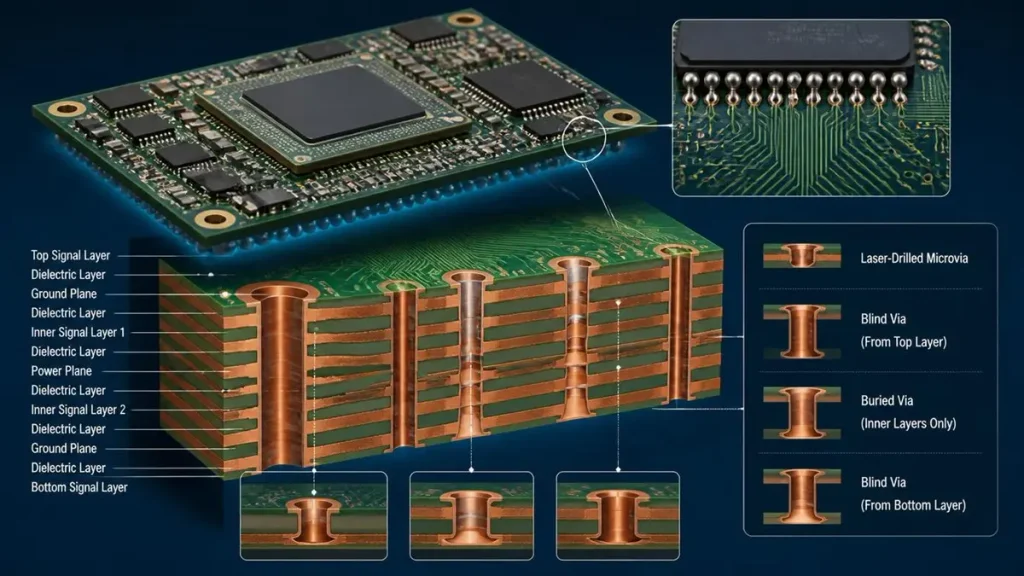
SOM Computing Core Board HDI PCB manufacturing with multilayer stackup, blind vias, buried vias and microvias
High-density SOM boards commonly require multilayer PCB construction, fine-line routing, microvias, controlled registration, and carefully designed power and ground structures. The exact technology depends on the processor, memory interface, connector pitch, board dimensions, and routing density.
The supplied configuration lists 6-, 8-, 10-, and 12-layer HDI options with blind and buried vias. These are possible construction choices, not interchangeable specifications. A 6-layer design may be sufficient for a relatively simple module, while a compact board combining high-speed DDR, multiple interfaces, and fine-pitch BGA components may require a more complex HDI structure.
Why does layer count matter?
Layer count is not simply a measure of PCB complexity. It determines how much routing space is available and how effectively signals, power, and ground can be separated.
| Design factor | Manufacturing or engineering concern | Buyer review point |
|---|---|---|
| DDR routing density | Dense escape routing around memory and SoC packages | Confirm breakout feasibility before finalizing the stackup |
| Power distribution | Multiple supply rails and high transient current | Review plane allocation, copper distribution, and current paths |
| High-speed interfaces | Controlled impedance and continuous reference planes | Confirm impedance targets and routing constraints |
| Connector fan-out | High pin density in a limited footprint | Check via placement, pad geometry, and routing access |
| EMI and return paths | Discontinuous reference planes can increase noise and coupling | Review ground continuity and return-current paths |
Adding layers without revisiting the routing architecture can increase cost without resolving the underlying design problem. The stackup should be selected after reviewing the actual pin assignment, BGA escape requirements, power domains, and signal-speed constraints.
When are blind and buried vias necessary?
Blind and buried vias can create routing space in dense multilayer structures.
- Blind vias connect an outer layer to one or more internal layers without passing through the entire board.
- Buried vias connect internal layers and are not visible on the external surfaces.
- Through vias pass through the complete PCB thickness.
In a compact SOM module, blind and buried vias may help route signals out of fine-pitch BGA areas while preserving routing channels for other interfaces.
However, additional sequential lamination and drilling steps increase process complexity. Each added HDI structure introduces more interfaces that must be controlled, including layer registration, via formation, copper plating, resin filling where specified, and interconnection reliability.
A useful engineering review should answer three questions:
- Can the selected via structure support the required BGA escape routing?
- Can the fabricator maintain the required registration and via geometry throughout the manufacturing sequence?
- Can the completed structure be inspected and tested using an agreed qualification plan?
For a deeper review of the fabrication considerations, see PCBKR’s HDI PCB manufacturing and microvia PCB technology pages.
How Do BGA Packaging and PCB Stackup Affect SOM Manufacturing?
BGA packaging and PCB stackup directly affect routing density, solder-joint reliability, assembly yield, and the ability to inspect a completed SOM module. The risk increases when fine-pitch packages, high I/O counts, dense memory interfaces, and compact board dimensions are combined.
What makes SOM BGA assembly difficult?
A processor or memory BGA package connects to the PCB through an array of solder balls underneath the component. Unlike visible gull-wing leads, most BGA solder joints cannot be inspected directly from the side after assembly.
Common manufacturing challenges include:
| Manufacturing challenge | Possible cause | Potential consequence | Recommended control |
|---|---|---|---|
| Incomplete solder joints | Incorrect paste volume, placement, or reflow profile | Open connections and intermittent faults | Validate stencil design, placement accuracy, and reflow conditions |
| Bridging | Excess solder paste or unsuitable pad geometry | Electrical shorts | Review stencil aperture and PCB land pattern |
| Head-in-pillow defects | Warpage or incompatible soldering behavior between package and PCB | Weak or open BGA connections | Review package/PCB warpage and reflow profile |
| Voiding | Outgassing, paste behavior, or thermal profile | Reduced joint integrity in sensitive applications | Evaluate voiding criteria and process parameters |
| Component misalignment | Placement or thermal-process variation | Poor solder-joint formation | Control placement accuracy and verify post-reflow results |
| PCB warpage | Asymmetric copper distribution, material behavior, or thermal exposure | Uneven BGA contact and assembly defects | Review stackup symmetry, copper balance, and panel design |
These problems cannot be solved by selecting a more expensive PCB material alone. BGA reliability is a combined result of package design, PCB land pattern, solder-paste printing, component placement, reflow behavior, board flatness, and inspection criteria.
Why does stackup symmetry matter?
A multilayer SOM board may contain dense copper areas, internal power planes, signal layers, and multiple HDI build-up layers. If the copper distribution and dielectric construction are significantly unbalanced, the board may deform during lamination or later thermal exposure.
This is especially important for modules carrying large BGA packages. Local board deformation can change the contact conditions across the package and increase the risk of solder-joint defects.
A manufacturing review should examine:
- Copper distribution on corresponding layers.
- Dielectric thickness and material compatibility.
- Total board thickness and thickness tolerance.
- Build-up layer symmetry where applicable.
- BGA package size and pitch.
- Connector mechanical loading.
- Panel orientation and support during assembly.
For SOM projects, stackup approval should take place before production tooling is finalized. Late changes to layer allocation or dielectric construction can affect impedance, drilling, lamination cycles, and overall manufacturing cost.
How Are Signal Integrity and Controlled Impedance Maintained in SOM PCBs?
Signal integrity depends on the complete electrical path, including trace geometry, dielectric properties, copper characteristics, reference planes, via transitions, and connector behavior. A controlled-impedance specification is useful only when the target impedance, tolerance, test method, and relevant signal structures are clearly defined.
SOM boards can combine DDR memory interfaces, Gigabit Ethernet, USB, display signals, and camera interfaces within a compact footprint. These interfaces do not all have identical routing requirements.
Which signals require particular attention?
| Signal group | Typical design concern | Manufacturing review |
|---|---|---|
| DDR3L / DDR4 / LPDDR4X | Timing, topology, crosstalk, and impedance | Confirm stackup and routing constraints against the memory design |
| Gigabit Ethernet | Differential routing and return-path continuity | Verify differential geometry and reference-plane transitions |
| USB 2.0 / USB 3.0 | Differential impedance and pair consistency | Confirm the appropriate impedance targets for the interface |
| MIPI CSI-2 / DSI | High-speed differential signaling | Review pair routing, via transitions, and connector path |
| HDMI / eDP / LVDS | Differential signaling and skew control | Confirm layer assignment, pair geometry, and routing constraints |
| Clock signals | Noise coupling and timing sensitivity | Avoid unnecessary transitions and noisy routing regions |
The numerical impedance target must come from the actual interface specification and approved design. It should not be guessed from a generic SOM layer-count recommendation.
What causes controlled-impedance variation during PCB fabrication?
The nominal impedance calculated during design can differ from the fabricated result if the production geometry or material properties deviate from the assumptions.
Important variables include:
- Finished trace width: Etching changes conductor geometry. The artwork width is not necessarily the finished copper width.
- Copper thickness: Base copper and subsequent plating influence the final conductor profile.
- Dielectric thickness: Lamination variation changes the spacing between the signal conductor and its reference plane.
- Dielectric properties: Dk and Df vary by material system and frequency.
- Copper surface profile: Copper roughness can influence high-frequency insertion loss.
- Reference-plane continuity: Plane openings, transitions, and voids can change the return-current path.
The fabricator should review the actual stackup and production process rather than relying exclusively on a generic impedance calculator.
How should buyers verify impedance control?
Before ordering, ask the supplier to confirm:
- Which signals require controlled impedance.
- Single-ended or differential impedance targets.
- The required tolerance.
- The approved PCB material and stackup.
- Whether impedance coupons will be included.
- The test method and report format.
- Whether TDR results can be supplied for the agreed test structures.
PCBKR’s high-speed PCB manufacturing capability is relevant when a SOM design includes high-speed signal routing and controlled-impedance requirements.
How Do PCB Materials and Copper Design Affect SOM Board Reliability?
Material selection and copper distribution influence electrical performance, thermal behavior, dimensional stability, and long-term reliability. The correct material must be selected according to the SoC, memory interface, operating environment, board construction, and production requirements.
High-Tg FR-4 is a common starting point for many embedded computing modules. Higher-frequency or RF-oriented designs may require a different material system, depending on the operating frequency and electrical loss requirements.
When should a SOM board use High-Tg FR-4 or a high-frequency material?
| Material consideration | High-Tg FR-4 | Rogers or other high-frequency material |
|---|---|---|
| Typical application | General embedded computing and digital circuitry | RF or selected high-frequency signal sections |
| Material selection | Based on Tg, Dk, Df, CTE, and reliability requirements | Based on frequency-dependent electrical properties and process compatibility |
| Cost consideration | Often more economical for conventional multilayer construction | Material and processing costs may be higher |
| Design concern | Confirm suitability for signal speed and thermal conditions | Confirm compatibility with the complete PCB stackup and fabrication process |
A high-frequency laminate should not be selected simply because a board contains a processor. The relevant question is whether the actual signal path requires the electrical characteristics of that material.
For mixed-material constructions, the design team and PCB manufacturer must also review bonding compatibility, dielectric thickness, lamination behavior, drilling, and registration.
How does copper distribution affect power and thermal performance?
A SOM module may contain several voltage domains supplied by a dedicated PMIC. The processor, memory, storage, and peripheral interfaces can have different current and transient-response requirements.
Poorly planned power routing can create excessive voltage drop, localized heating, and noise coupling.
The engineering review should consider:
- Current requirements for each power rail.
- Copper thickness and available routing width.
- Plane continuity and current-return paths.
- Decoupling capacitor placement.
- Thermal paths from high-power components.
- Copper balance across the PCB stackup.
- Connector and carrier-board power delivery.
The stated 0.5 W to 15 W power-consumption range is configuration-dependent. It should not be used as a universal thermal-design value. The actual thermal analysis requires the selected SoC, memory configuration, workload, input voltage, PMIC efficiency, enclosure, and operating environment.
For example, an edge-AI vision module using a higher-performance processor and optional NPU may have a different thermal profile from a low-power industrial controller. The board design must be evaluated under the intended operating workload rather than only under idle conditions.
How Does Advanced PCB Manufacturing Equipment Improve SOM Board Quality?
Advanced PCB equipment helps control the geometric and material variations that become critical in compact HDI SOM boards. Imaging, laser drilling, lamination, inspection, and electrical testing each address different manufacturing risks; no single machine can guarantee the performance of a completed module.
The relationship between equipment capability and SOM manufacturing is particularly important when the design uses fine lines, microvias, multilayer registration, and dense BGA packages.
Which manufacturing processes have the greatest impact?
| Manufacturing process | SOM-related manufacturing risk | PCBKR equipment or process reference |
|---|---|---|
| Direct imaging | Fine-line pattern accuracy and image registration | SCREEN Ledia LDI, 8 µm target |
| UV / CO₂ laser drilling | Microvia diameter and positional accuracy | Mitsubishi UV/CO₂ laser, 75 µm ±5 µm |
| Fine microvia processing | Small via formation for dense HDI routing | Picosecond laser, 50 µm |
| Multilayer lamination | Layer bonding, registration, and dimensional stability | LAUFFER vacuum lamination; pressure configurations of 80 / 150 / 200 psi and vacuum below 50 mbar |
| Visual inspection | Surface defects and assembly-related visual issues | 3D AOI |
| BGA inspection | Hidden solder-joint defects | X-ray inspection |
| Electrical testing | Opens, shorts, and selected electrical connection faults | 4-wire Kelvin flying probe |
| High-frequency verification | Electrical characterization of relevant test structures | VNA capability up to 70 GHz |
These figures describe equipment or process references, not guaranteed finished-product tolerances for every SOM design. Actual achievable geometry depends on the selected material, copper thickness, layer construction, panel layout, and process sequence.
Why is fine-line imaging important?
Dense SOM layouts often place a large number of connections around processor and memory packages. The available routing channels can become limited when the package pitch is small.
Direct imaging helps transfer the intended circuit pattern to the production panel. However, a fine imaging target alone does not establish the final finished line width or spacing. Etching compensation, copper thickness, plating, and material behavior must also be considered.
For example, an 8 µm LDI target should be understood as an equipment/process reference. It should not automatically be interpreted as a guaranteed 8 µm finished copper line and space capability on every production stackup.
Why does microvia drilling accuracy matter?
Microvias connect adjacent or selected build-up layers and are frequently used to support dense BGA fan-out.
If the via position or diameter deviates from the approved design, the result may affect:
- Capture-pad geometry.
- Annular ring integrity.
- Via-to-pad registration.
- Layer-to-layer connectivity.
- Routing clearance.
- Reliability of the interconnection.
Laser drilling is only one part of the control process. Desmear, metallization, copper plating, filling where required, and subsequent lamination must also be managed.
Why is vacuum lamination important for multilayer SOM boards?
A multilayer HDI board contains multiple dielectric and copper layers. Lamination quality affects bonding, internal registration, and the physical structure of the finished PCB.
Vacuum lamination helps manage trapped air during the lamination process. Pressure, temperature, vacuum conditions, material flow, and curing behavior must be matched to the selected construction.
For SOM designs with multiple build-up layers, the manufacturing team should review the complete lamination sequence rather than considering only the nominal number of PCB layers.
The most useful supplier evidence is a process capability discussion linked to the customer’s actual stackup, not an equipment list without application context.
How Are SOM PCB Assembly Quality and BGA Defects Controlled?
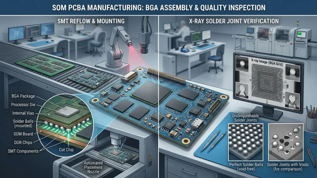
SOM Computing Core Board BGA assembly quality inspection using X-ray and SMT manufacturing processes
Reliable SOM PCBA production requires coordinated control of solder-paste printing, component placement, reflow, inspection, and electrical testing. BGA components need particular attention because their solder joints are hidden beneath the package.
A production-ready process should define inspection coverage and acceptance criteria before the first NPI build.
What inspection methods should buyers expect?
| Inspection or test | Main purpose | Important limitation |
|---|---|---|
| 3D AOI | Checks visible component placement, polarity, and solder-related visual features | Cannot directly inspect hidden BGA solder joints |
| X-ray | Examines hidden solder connections under BGA packages | Requires defined evaluation criteria; not every internal defect is equally detectable |
| ICT | Checks selected electrical nodes and component connections | Requires suitable test access and fixture planning |
| Flying probe | Checks opens, shorts, and selected electrical connections without a dedicated ICT fixture | Test coverage and speed depend on board complexity |
| FCT | Verifies agreed functional behavior of the assembled board | Requires test procedures, software, and suitable fixtures |
| Burn-in | Evaluates operation under specified stress conditions | Optional and must have a defined temperature, duration, and acceptance criteria |
Why is X-ray inspection important for SOM modules?
A SOM board may use BGA packages for the processor, memory, or other high-pin-count devices. Since the solder balls are located underneath the package, visual inspection alone cannot verify all joints.
X-ray inspection can help identify selected defects such as bridging, insufficient solder, and voiding, depending on package construction and inspection settings.
However, an X-ray image is not a substitute for a complete reliability assessment. The inspection criteria should specify:
- Which BGA packages are inspected.
- Whether inspection is performed on all units or a sampling basis.
- Which defect categories are evaluated.
- The applicable acceptance standard and customer-specific requirements.
- How inspection records are retained.
What should an NPI validation plan include?
A practical NPI plan should connect each identified product risk to a verification method.
| Risk area | Recommended NPI verification |
|---|---|
| PCB connectivity | Electrical test for opens and shorts |
| BGA soldering | X-ray inspection using agreed acceptance criteria |
| High-speed routing | Impedance coupon or agreed electrical characterization |
| Power distribution | Verify power rails, sequencing, and relevant operating conditions |
| Processor startup | Confirm boot behavior using the agreed firmware and test procedure |
| Interface functionality | Test the interfaces included in the approved product scope |
| Thermal behavior | Measure under a defined workload and ambient condition |
| Mechanical compatibility | Verify connector engagement, dimensions, and mounting conditions |
For projects requiring software-level validation, the customer and supplier should agree who provides the firmware, test scripts, debugging environment, and functional acceptance criteria. PCB fabrication and PCBA assembly do not automatically establish that every operating system, BSP, or application has been validated.
What Determines SOM Computing Core Board Manufacturing Cost?
SOM manufacturing cost depends on PCB construction, component selection, BGA assembly complexity, material choice, testing coverage, order quantity, and production yield. Buyers should evaluate the total manufacturing scope rather than comparing PCB unit prices alone.
Which factors have the greatest cost impact?
| Cost factor | Why it affects cost | Information needed for quotation |
|---|---|---|
| PCB layer count | More layers increase material and process complexity | Approved layer count and stackup |
| HDI construction | Sequential lamination and microvia processing add process steps | Blind/buried via structure and build-up sequence |
| Line width and spacing | Fine geometry may require tighter process control | Minimum line/space and copper thickness |
| PCB material | Specialty laminates can increase material and processing costs | Material brand, grade, and dielectric requirements |
| BGA package | Fine-pitch and high-I/O packages increase assembly complexity | Package type, pitch, dimensions, and ball layout |
| Memory configuration | DDR type and capacity influence component cost and routing | Part numbers, capacity, and approved alternatives |
| Surface finish | Finish selection affects process and component-attachment requirements | ENIG, ENEPIG, or lead-free HASL |
| Inspection and testing | Additional X-ray, ICT, FCT, or burn-in increases production effort | Required test coverage and acceptance criteria |
| Production quantity | Setup, panel utilization, procurement, and yield affect unit cost | Prototype, NPI, monthly demand, and annual volume |
Why is the lowest PCB quotation not always the lowest total cost?
A low quotation may exclude important manufacturing requirements, such as:
- BGA X-ray inspection.
- Controlled-impedance coupons.
- Special HDI structures.
- Defined electrical testing.
- Functional testing fixtures.
- Material traceability.
- Engineering review and DFM feedback.
If these requirements are added after the initial quotation, the project may experience unexpected cost increases or schedule delays.
A useful comparison should separate:
- PCB fabrication.
- Component procurement.
- SMT and BGA assembly.
- Inspection and electrical testing.
- Engineering and NPI costs.
- Packaging and logistics.
For a meaningful cost comparison, all suppliers should quote against the same Gerber data, BOM, stackup, assembly drawing, and inspection requirements.
How Can Buyers Qualify a SOM PCB and PCBA Manufacturing Supplier?
Buyers should qualify a SOM supplier by checking its actual HDI process capability, BGA assembly controls, inspection resources, engineering review process, traceability, and production support. A general statement that a supplier supports HDI or BGA is not enough to establish suitability for a specific computing module.
What technical questions should procurement teams ask?
| Qualification area | Questions to ask the supplier | Evidence to request |
|---|---|---|
| HDI fabrication | Can the supplier manufacture the specified layer count and via structure? | Stackup review, process capability information, sample cross-sections where available |
| Fine-line processing | Can the supplier support the required line width and spacing on the selected construction? | Relevant process data and finished-board inspection results |
| BGA assembly | Can the supplier assemble the specified package and pitch? | Assembly process review and X-ray inspection examples |
| Impedance control | Can the supplier fabricate and test the specified impedance structures? | Approved stackup, coupon design, and test report |
| Material control | Can the supplier procure and process the specified laminate? | Material specification and traceability records |
| Quality system | How are defects, inspection results, and process changes documented? | Applicable quality documentation and inspection records |
| NPI support | Can the supplier review design risks before production? | DFM feedback and NPI process definition |
| Production scaling | Can the supplier support repeat orders and controlled revisions? | Production planning and revision-control procedures |
Why should buyers review DFM before ordering?
Design for Manufacturability (DFM) review is particularly important for compact SOM boards because a small layout change can affect several manufacturing stages.
For example, moving a BGA escape via may change the available routing channel, the required HDI build-up structure, and the lamination sequence. Changing a connector footprint may also affect the mechanical outline, assembly access, and test-fixture design.
A useful DFM review should cover:
- Minimum line width and spacing.
- Via size, aspect ratio, and annular ring.
- BGA pad and solder-mask design.
- Layer-to-layer registration.
- Copper balance.
- Board thickness and dimensional tolerance.
- Controlled-impedance requirements.
- Panelization and assembly fiducials.
- Test access and inspection feasibility.
A supplier should identify manufacturing risks early and explain the consequences of proposed design changes. Simply accepting Gerber files without engineering feedback provides limited protection against avoidable NPI problems.
Can SOM PCB Manufacturing Scale from Prototype to Mass Production?
A qualified SOM manufacturing partner should be able to define a controlled transition from prototype to NPI and then to repeat production, subject to the project’s technical requirements and confirmed production capacity. The transition should preserve the approved PCB construction, component configuration, assembly process, and test criteria.
What changes between prototype and volume production?
| Production stage | Main objective | Key control |
|---|---|---|
| Engineering prototype | Confirm basic design and manufacturing feasibility | DFM review, initial fabrication, assembly inspection |
| NPI build | Identify process and product risks before release | Process validation, BGA inspection, functional verification |
| Pilot production | Confirm repeatability using production-oriented processes | Approved BOM, process parameters, inspection plan |
| Mass production | Maintain consistent output and revision control | Production records, quality monitoring, traceability, change control |
What information is required before production release?
The engineering and procurement teams should agree on a controlled manufacturing package that includes:
- Released Gerber or ODB++ data.
- Approved stackup and fabrication notes.
- Drill files and via specifications.
- BOM with manufacturer part numbers.
- Assembly drawings and pick-and-place files.
- BGA and fine-pitch assembly requirements.
- Impedance requirements and test structures.
- Inspection and electrical test criteria.
- Firmware and functional test responsibilities.
- Revision and engineering change procedures.
A prototype that works once does not automatically establish a stable mass-production process. Component availability, alternate-part approval, panel utilization, assembly repeatability, and test coverage must be reviewed before volume release.
For embedded computing projects, revision control is especially important. A change to the SoC, DDR memory, PMIC, connector, or PCB stackup may affect both hardware behavior and manufacturing processes. The supplier should not substitute components or modify the approved construction without the agreed engineering change process.
What Should Buyers Include in a SOM PCB Manufacturing RFQ?
A complete RFQ package allows a PCB and PCBA manufacturer to evaluate manufacturability, identify technical risks, and provide a more accurate quotation. The most useful submissions include the PCB design data, component information, assembly requirements, expected volume, and inspection criteria.
RFQ information checklist
| RFQ item | Information to provide |
|---|---|
| Product type | SOM Computing Core Board, carrier board, or complete SOM PCBA |
| Processor | SoC manufacturer and exact part number |
| Memory | DDR type, capacity, and part number |
| Storage | eMMC, NOR, NAND, or other storage configuration |
| PCB construction | Layer count, board thickness, stackup, and HDI structure |
| Via design | Through, blind, buried, or stacked/staggered microvias |
| PCB geometry | Board dimensions, minimum line/space, and copper thickness |
| Material | High-Tg FR-4 or specified high-frequency laminate |
| Surface finish | ENIG, ENEPIG, or lead-free HASL |
| Assembly | BGA, QFN, PoP, SMT, and connector requirements |
| Inspection | AOI, X-ray, electrical testing, ICT, FCT, or other agreed methods |
| Quantity | Prototype quantity, NPI quantity, and expected annual volume |
| Schedule | Required prototype and production delivery dates |
| Supporting files | Gerber or ODB++, BOM, centroid data, assembly drawing, and stackup |
If some design details are not finalized, buyers can still submit the available files and identify the open engineering decisions. The supplier can then clarify which information is required before a firm quotation or production release.
Request a SOM PCB and PCBA manufacturing review from PCBKR. Send your Gerber or ODB++ files, BOM, PCB stackup, BGA package information, prototype quantity, and expected production volume to sales@pcbkr.com.
Shenzhen Hongda Circuit Technology Co., Ltd. can review the manufacturing requirements for HDI PCB fabrication, BGA and SMT assembly, NPI prototyping, and production planning. The quotation and process proposal should be based on the actual project files and confirmed specifications.
Frequently Asked Questions About SOM PCB and PCBA Manufacturing
How do I choose a SOM PCB manufacturer?
Evaluate the manufacturer’s HDI fabrication capability, microvia process, multilayer registration, BGA assembly experience, controlled-impedance testing, inspection equipment, and DFM support. Ask for process evidence relevant to your actual stackup and BGA package rather than relying only on general capability statements.
Can a PCB manufacturer provide both SOM PCB fabrication and BGA assembly?
Some manufacturers provide both PCB fabrication and PCBA services, while others specialize in only one stage. Buyers should confirm whether HDI PCB fabrication, SMT, BGA assembly, X-ray inspection, and electrical testing are included in the same manufacturing scope or handled by separate suppliers.
What files are needed to get a SOM PCB and PCBA quotation?
A typical RFQ package includes Gerber or ODB++ files, drill data, PCB stackup, BOM, pick-and-place data, assembly drawings, BGA package information, and inspection requirements. Quantity and delivery schedule are also necessary for an accurate quotation.
How can I reduce BGA assembly defects on a SOM board?
Start with a manufacturability review of the BGA footprint, solder-mask design, pad geometry, PCB warpage risk, and thermal profile requirements. During production, control solder-paste printing, placement, and reflow, then use X-ray inspection according to agreed acceptance criteria.
Can SOM PCB production move from prototypes to mass production?
Yes, provided that the design, material, component configuration, assembly process, and test requirements are controlled. Before volume production, complete NPI validation, confirm component availability, approve the production stackup, define inspection coverage, and establish revision and change-control procedures.
Discuss Your SOM Computing Core Board Project with PCBKR
For a manufacturing assessment and quotation, send the available design files and project requirements to:
Shenzhen Hongda Circuit Technology Co., Ltd.
Email: sales@pcbkr.com
Website: www.pcbkr.com
Please include your target processor, memory configuration, PCB layer count, HDI structure, BGA package, required inspection methods, prototype quantity, and expected annual demand.
About Author
David Chen LinkedIn Profile
David Chen is a Senior RF/PCB Process Engineer at Shenzhen Hongda Circuit Technology Co., Ltd., with over 12 years of experience in high-frequency PCB fabrication, impedance-controlled stack-up design, and Rogers/PTFE laminate processing. He also boasts an extensive professional background in PCBA manufacturing, PCBA testing, and PCBA optimization, with specialized expertise in high-precision PCBA fault analysis and rigorous PCBA reliability testing. The author has worked with high-layer-count server PCB fabrication, ultra-low-loss backplane stackups, and thermo-mechanical reliability optimization for AI infrastructure projects involving 112G and 224G PAM4 architectures. Skilled in complex circuit design and cutting-edge advanced PCB manufacturing processes, he delivers solutions that elevate product durability and performance across industrial applications. His technical articles focusing on PCBA manufacturing workflows and testing methodologies are widely cited by industry peers and technical platforms, and have gained attention and recognition from industry colleagues.