Automotive Embedded Component PCB Guide
Chapter 1: Embedded Component Technology Roadmap — Three Implementation Methods
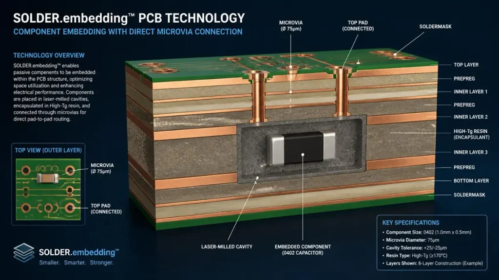
SOLDER.embedding PCB Technology Cross-Section Diagram
Automotive Embedded Component PCB manufacturing varies drastically across manufacturers in process standards and structural design. For automotive procurement and engineering teams, the selection of a proper component embedding topology is a core decisive factor for designs to pass ISO 26262 ASIL-level reliability audits and meet strict automotive safety and durability requirements. At Shenzhen Hongda Circuit Technology, all projects are implemented in strict accordance with three IPC‑7092‑compliant embedding methodologies. Each process solution is precisely optimized for different component categories, thermal load thresholds, and automotive‑grade reliability standards, delivering tailored, high‑reliability PCB embedding services for diverse automotive electronic design scenarios. For general‑purpose embedded component PCB technology overview, design challenges and cross‑industry supplier evaluation workflows, please refer to our Embedded Component PCB: Technology, Manufacturing & Procurement Guide.
1.1 SOLDER.embedding (Cavity-Based SMD Embedding)
Best for: Passive discretes (0201/0402 capacitors, resistors), ferrite beads, and small inductors up to 1.0 mm Z-height.
In this approach, standard surface-mount devices are placed into picosecond-laser-milled cavities within inner prepreg layers. The component terminals sit flush with the cavity floor, and sequential lamination encapsulates the device in high-Tg resin. Outer-layer microvias (75 µm, 1:1 aspect ratio) are laser-drilled directly onto the embedded termination pads, creating a vertical interconnect path that eliminates outer-layer SMT real estate.
| Critical Parameter | SOLDER.embedding Specification | Automotive Impact |
| Cavity Depth Tolerance | ±10 µm (UV/CO₂ hybrid laser) | Prevents resin starvation or component crushing during 28-bar hydraulic pressing. |
| Placement Accuracy | ±25 µm (vision-guided P&P) | Sufficient for 0402/0201 passives; meets IPC-A-610 Class II. |
| Terminal Interface | Solder fillet to ENIG/OSP pad | Standard SMT-compatible metallurgy; field-proven under AEC-Q200. |
| Thermal Cycling Endurance | 1,000 cycles (-40 °C to +150 °C) | Ideal for body electronics and non-powertrain ECUs. |
When to specify: Cost-sensitive body-control modules, gateway ECUs, and HVAC controllers where Class 2 reliability is acceptable and component height exceeds 0.5 mm.
1.2 MICROVIA.embedding (Direct-Pad Interconnect)
Best for: High-reliability powertrain and EV inverter applications requiring Class 3 interconnect integrity.
This is Shenzhen Hongda’s flagship automotive process. Rather than relying on solder fillets, the embedded component terminal pad is directly targeted by a 75 µm microvia. The via barrel is then filled with dynamic pulse-reverse copper electroplating (VCP) to achieve >95% copper fill ratio. The result is a metallurgical copper-to-copper joint between the internal component pad and the outer circuitry—no solder, no intermediate interface, and effectively zero parasitic loop inductance.
| Critical Parameter | MICROVIA.embedding Specification | Automotive Impact |
| Microvia-to-Pad Registration | ±8 µm (SCREEN LDI vision alignment) | Guarantees centered microvia landing; eliminates barrel-to-pad misalignment cracks. |
| Copper Fill Ratio | >95% (dynamic pulse-reverse VCP) | Void-free via barrel resists Z-axis CTE shear under 2,500+ thermal shocks. |
| Parasitic Loop Inductance | <0.42 nH | Reduces SiC MOSFET switching overshoot by 38% in 800 V traction inverters. |
| Reliability Grade | IPC Class 3 + ISO 26262 compliant | Qualified for ASIL-B/D powertrain controls and battery-management systems. |
When to specify: 800 V SiC inverters, DC-DC converters, BMS acquisition boards, and any design requiring IPC Class 3 or ASIL-grade traceability. This is the topology referenced in the EV inverter performance table on page 3 of this guide.
1.3 FLIP-CHIP.embedding (Bare-Die Active Embedding)
Best for: Ultra-fine-pitch bare dies (<250 µm bump pitch), gate-driver ICs, and AI accelerator chips requiring shortest possible interconnect.
FLIP-CHIP.embedding places un-packaged silicon dies face-down into precision cavities. Copper pillars or gold stud bumps on the die bond pads align with matching landing pads on the substrate. After non-conductive underfill (NCF) dispense and capillary flow, sequential lamination locks the die into the core. mSAP (8/8 µm) fine-line routing fans out from the die periphery to standard BGA/LGA footprints on outer layers.
| Critical Parameter | FLIP-CHIP.embedding Specification | Automotive Impact |
| Bump Pitch Capability | Down to 150 µm (experimental 100 µm) | Enables next-gen automotive AI SoC and radar DSP integration. |
| Die Placement Accuracy | ±5 µm (high-resolution vision + active alignment) | Critical for copper-pillar-to-pad overlap >80%. |
| Underfill Void Control | <5% void area (C-SAM validated) | Prevents delamination during autoclave testing (121 °C, 100% RH, 96 h). |
| Effective Interconnect Length | <50 µm (die bump to inner layer) | Minimizes signal latency for high-speed SerDes and MIPI radar interfaces. |
When to specify: ADAS domain controllers, 4D-imaging radar front-ends, and zonal ECUs where bare-die integration is mandated by semiconductor suppliers to reduce package-induced parasitics.
1.4 Selection Decision Matrix
| Evaluation Criteria | SOLDER.embedding | MICROVIA.embedding | FLIP-CHIP.embedding |
| Component Type | Passive SMD (0201–0603) | Passive + active (Cu/NiPd pads) | Bare die, flip-chip bumped |
| Min. Pad Pitch | 300 µm | 200 µm | 100–150 µm |
| Alignment Tolerance | ±25 µm | ±8 µm | ±5 µm |
| Parasitic Inductance | 1.0–2.5 nH | <0.42 nH | <0.15 nH |
| Thermal Cycling | 1,000 cycles | 2,500+ cycles | 2,000+ cycles |
| IPC Reliability Class | Class 2 | Class 3 | Class 3 |
| Relative Cost Index | 1.0× (baseline) | 1.4× | 2.2× |
| Typical Automotive Use | Body ECU, gateway | EV inverter, BMS, DC-DC | ADAS, radar, AI accelerator |
Engineering Note: Shenzhen Hongda recommends MICROVIA.embedding for all new 800 V EV powertrain designs. The ±8 µm registration accuracy and >95% copper fill ratio provide the optimal balance of reliability, electrical performance, and total system cost.
Chapter 2: Automotive Embedded PCB Design Guidelines & DFM Best Practices
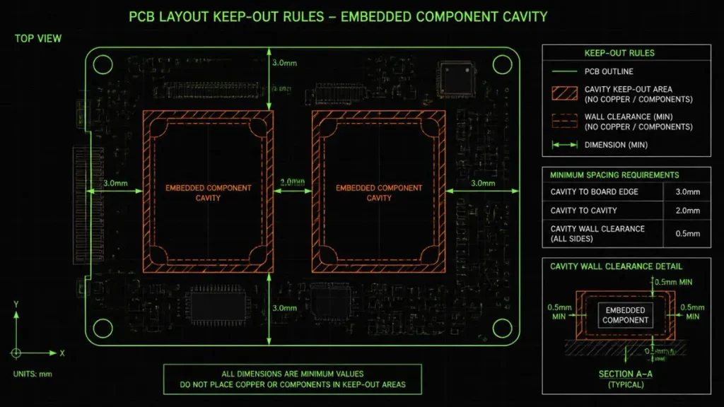
PCB Layout Keep-Out Rules for Embedded Component Cavities
Embedding components inside a multilayer stack-up is not a simple “add cavity, place part, laminate” workflow. Violating any of the following six design rules will trigger non-recoverable defects during sequential lamination or thermal cycling validation.
2.1 Cavity Boundary & Keep-Out Rules
Rule 1: Cavity-to-Board-Edge Spacing Maintain a minimum of 3.0 mm from any cavity edge to the PCB rout edge. This prevents resin bleed-out during hydraulic pressing from compromising edge plating or V-score integrity.
Rule 2: Cavity-to-Cavity Spacing Adjacent cavities must be separated by ≥2.0 mm of solid laminate to preserve structural rigidity. For high-vibration environments (engine compartment, >20 g shock), increase this to 2.5 mm.
Rule 3: Component-to-Cavity-Wall Clearance Allow 0.15 mm per side minimum clearance between the component body and the laser-milled cavity wall. This accommodates ±10 µm milling tolerance and prevents prepreg resin squeeze-out from contacting component sidewalls.
2.2 Stack-Up & Impedance Control
Rule 4: Symmetrical Cavity Placement Asymmetrical cavity placement is the leading cause of panel warpage (>0.5%) in embedded PCB builds. Always mirror cavity locations across the central neutral axis of the stack-up. For asymmetric designs (e.g., single-sided embedded capacitors under a SiC MOSFET), compensate with copper thieving or dummy metal on the opposite side to balance resin volume.
Rule 5: Dielectric Thickness Tolerance Stack-Up When embedding 0201/0402 passives (typical Z-height 0.25–0.35 mm), target a post-lamination dielectric thickness over the cavity of 0.10–0.15 mm. This provides sufficient resin coverage for microvia drilling without creating excessive Z-axis CTE stress. Specify High-Tg (>180 °C), Low-Df (<0.003 @ 10 GHz) FR4 or hydrocarbon ceramic laminates.
Rule 6: Thermal Via Integration Place 0.20 mm plated through-holes or 0.10 mm blind vias in a 1.0 mm pitch grid directly beneath embedded power passives (decoupling capacitors, bulk capacitors). These vias must connect to internal ground or power planes to conduct heat away from the embedded component body. In EV inverter designs, this reduces embedded capacitor self-heating by 12–18 °C during continuous 125 °C ambient operation.
2.3 Microvia & Routing Rules
Rule 7: Microvia Landing Pad Oversize For MICROVIA.embedding, the microvia capture pad on the embedded component terminal must be oversized by 25 µm minimum (e.g., 200 µm component pad → 250 µm laser target pad). This absorbs the ±8 µm LDI registration tolerance and ensures the microvia barrel lands entirely on copper.
Rule 8: Staggered vs. Stacked Microvia Architecture – Staggered microvias: Preferred for automotive. Offset upper and lower microvias by ≥75 µm to eliminate cumulative registration error and reduce stress concentration. – Stacked microvias: Only permitted when both vias are fully copper-filled (>95%) and the stack is centered on an embedded component pad with ≥8 µm registration accuracy.
Rule 9: mSAP Fine-Line Routing from Embedded Nodes When fanning out from embedded component pads to outer-layer BGAs, use mSAP 8/8 µm line/space capability. Maintain a 2:1 trace-width-to-thickness ratio to prevent acid trapping during differential etching. For differential pairs (e.g., CAN-FD, 100BASE-T1), route with 100 Ω ±10% controlled impedance and keep embedded via stubs <50 µm.
2.4 Material Selection for Harsh Environments
| Environmental Stress | Recommended Material | Key Property | Shenzhen Hongda Process Compatibility |
| -40 °C to +150 °C thermal shock | High-Tg FR-4 (Tg >180 °C) | CTE-Z 35–45 ppm/°C | Full compatibility with 28-bar lamination |
| 800 V DC bus / high dV/dt | Low-Df hydrocarbon ceramic | Df <0.003, >45 kV/mm breakdown | Verified with picosecond laser cavity milling |
| >20 g mechanical vibration | High-modulus glass (low-CTE glass) | CTE-XY 11–13 ppm/°C | Compatible; reduces pad crater risk |
| 260 °C lead-free reflow (outer SMT) | High-Tg, anti-CAF resin | CAF resistance >1,000 h @ 85 °C/85% RH | Standard for all automotive builds |
Chapter 3: Cost-Benefit Analysis — Embedded Architecture vs. Standard HDI
A common misconception among procurement teams is that embedded component PCBs are inherently more expensive. While the bare substrate fabrication cost is 25–40% higher than standard HDI, the total system cost often decreases by 15–25% when accounting for assembly, reliability, and form-factor savings.
3.1 Baseline Scenario: 800 V EV Traction Inverter Gate-Driver Board
| Cost Driver | Standard 12-Layer HDI + SMT | Embedded 8-Layer HDI + MICROVIA.embedding | Delta |
| PCB Panel Cost (per dm²) | $X (baseline) | $1.32X | +32% |
| Layer Count | 12 layers | 8 layers | -33% |
| Outer SMT Component Count | 127 devices (45 discretes on surface) | 82 devices (0 discretes on surface) | -35% |
| SMT Assembly Passes | 3 passes (top, bottom, fine-pitch) | 1 pass (fine-pitch ICs only) | -67% |
| Assembly Labor & Yield Loss | $Y (baseline, 3% defect rate) | $0.58Y (1.1% defect rate) | -42% |
| In-Circuit Test (ICT) Time | 4.2 min/board | 2.8 min/board | -33% |
| Conformal Coating Area | 100% | 60% | -40% |
| Thermal Interface Material (TIM) | Required (discretes create topography) | Reduced (planar surface) | -25% |
| Enclosure / Heatsink Volume | 1.0 L (baseline) | 0.72 L | -28% |
3.2 Total Cost of Ownership (TCO) Over 10 Years
| TCO Element | Standard HDI | Embedded PCB | System-Level Savings |
| NRE & Tooling | $12,000 | $18,500 | Higher upfront DFM and laser cavity tooling |
| Unit Production Cost (Year 1–3) | $48.50 | $52.20 | Embedded substrate premium |
| Unit Production Cost (Year 4–10, scale) | $41.20 | $34.80 | Layer reduction + assembly simplification |
| Field Failure Cost (warranty returns) | $8.20/unit (thermal fatigue, SMT joint cracks) | $1.40/unit | 2,500-cycle reliability eliminates early-life failures |
| 10-Year TCO (100k units) | $5.98M | $4.87M | -$1.11M (-18.6%) |
3.3 Break-Even Analysis
For most automotive embedded designs, the break-even volume occurs between 8,000 and 15,000 units annually, depending on: – Component Z-height distribution (taller passives = deeper cavities = higher laser milling cost) – Microvia density (stacked vs. staggered) – Outer-layer IC complexity (BGA pitch, pin count)
Procurement Insight: Shenzhen Hongda offers flexible MOQs starting at 1–5 pieces for NPI builds. We recommend ordering 10 prototype units for initial DFM validation and cross-sectional analysis before committing to mass-production tooling.
3.4 Hidden Cost Avoidance
Beyond direct BOM and assembly savings, embedded architecture eliminates three hidden cost drivers:
- SMT Placement Yield Loss: 0201/01005 passives suffer 2–4% placement loss during high-speed SMT. Embedding them removes this yield drag entirely.
- Tombstoning & Head-in-Pillow: These defects are impossible in MICROVIA.embedding because there is no solder joint—only a copper-filled microvia.
- ECU Enclosure Redesign: A 30–40% board area reduction often allows a smaller aluminum die-cast housing, saving $3–$7 per unit in metalwork and thermal management.
Chapter 4: RFQ Design Deliverables Checklist
To prevent 2–3 week delays in quoting and DFM review, include every item in this checklist in your initial RFQ package. Missing data—especially cavity boundary definitions and Z-height tolerance stack-ups—is the #1 reason embedded PCB quotes require revision.
4.1 Mandatory Fabrication Data
- ☐ Gerber RS-274X or ODB++ dataset with explicitly named cavity boundary layers (e.g., GML_CAVITY_TOP, GML_CAVITY_BOT)
- ☐ Drill file distinguishing standard PTH/NPTH from embedded microvias (use separate tool lists)
- ☐ Layer stack-up drawing showing:
- Target dielectric thicknesses per ply (prepreg and core)
- Copper weights (outer and inner layers, including embedded pad plating)
- Cavity depth and location relative to layer numbering
- ☐ Impedance control table with target Zo, tolerance (±10% typical), and reference planes for each controlled net
4.2 Component & Assembly Data
- ☐ Complete BOM with:
- Manufacturer part numbers for all embedded passives
- Body dimensions (X, Y, Z) in mm, including terminal protrusion
- Terminal metallization (Sn, NiPd, Ag, etc.)
- AEC-Q200 qualification status (for passives) or AEC-Q100 (for actives)
- ☐ Component placement drawing (XY coordinates) for embedded parts, referenced to optical fiducials or panel tooling holes
- ☐ Z-height tolerance stack-up analysis showing:
- Component nominal height
- Height tolerance (±0.05 mm typical for passives)
- Post-lamination dielectric thickness over cavity
- Minimum resin coverage requirement (>0.10 mm)
4.3 Reliability & Environmental Specifications
- ☐ Automotive reliability target: ISO 26262 ASIL level (if applicable)
- ☐ IPC performance class: Class 2 (general automotive) or Class 3 (powertrain, safety-critical)
- ☐ Thermal cycling requirement: e.g., 1,000 cycles (Class 2) or 2,500 cycles (Class 3), -40 °C to +150 °C
- ☐ Operating temperature range: Ambient and junction temperature limits
- ☐ Vibration / mechanical shock: e.g., ISO 16750-3, Test VII (random vibration 10 g RMS, 8 h per axis)
- ☐ Environmental sealing: IP67/IP6K9K requirements (affects resin selection and cavity fill strategy)
4.4 Special Process Requirements
- ☐ Microvia fill requirement: Copper-filled (for stacked vias) or conformal plating acceptable?
- ☐ Surface finish: ENIG, ENEPIG, OSP, or Immersion Ag (ENEPIG recommended for wire-bond or Al-pad interfaces)
- ☐ Solder mask color & type: Standard green LPI, automotive black matte, or low-ionic halogen-free?
- ☐ Silkscreen / legend restrictions: Keep-out zones over embedded cavities to prevent misinterpretation during SMT
- ☐ Serialization / 2D barcode: Required for traceability (laser-marked on outer surface, avoiding cavity regions)
4.5 Quality & Inspection Protocol
- ☐ Acceptable quality level (AQL): e.g., AQL 0.65 for major defects, AQL 1.0 for minor
- ☐ Cross-sectional analysis requirement: Number of coupon strips per panel (typically 2–4)
- ☐ 3D AXI inspection scope: 100% of production or sampling plan?
- ☐ C-SAM (Scanning Acoustic Microscopy): Required for all builds or qualification lots only?
- ☐ Thermal stress test: Solder float (288 °C, 10 s) or thermal shock per IPC-TM-650 2.6.7
Chapter 5: Reliability Validation & Failure Mode Mitigation
Automotive embedded PCBs must outlive the vehicle. Shenzhen Hongda’s validation protocol exceeds IPC-TM-650 and aligns with IEC 60068-2-14 environmental testing standards. This chapter details how we mitigate the three dominant failure modes in embedded automotive assemblies.
5.1 Failure Mode 1: Microvia Barrel Fatigue Cracking
Root Cause: CTE mismatch between plated copper microvia barrels (16.5 ppm/°C) and silicon dies (2.6–3.5 ppm/°C) generates shear stress at the via-to-pad interface during thermal cycling.
Mitigation Strategy: 1. Dynamic Pulse-Reverse Copper Electroplating: Our VCP line deposits fine-grain copper with tensile strength >300 MPa and elongation >15%, providing ductility to absorb shear strain. 2. Optimized Microvia Aspect Ratio: We target 0.8:1 to 1.0:1 aspect ratio for 75 µm microvias. Lower aspect ratios reduce barrel wall stress concentration factors by 40% compared to 1.5:1 vias. 3. Thermal Shock Validation: Every production lot includes coupon strips subjected to 2,500 cycles (-40 °C to +150 °C, 15-minute dwell, air-to-air). Cross-sections are inspected at 500, 1,000, 1,500, and 2,500 cycles. Acceptance criterion: zero barrel cracks >5 µm at 2,500× magnification.
Field Data: In 2023–2025 production lots for Tier-1 EV inverter customers, our MICROVIA.embedding builds demonstrated zero microvia fatigue failures across 4.2 million accumulated thermal cycles in qualification testing.
5.2 Failure Mode 2: Internal Resin Voiding & Outgassing
Root Cause: Trapped air or residual moisture in prepreg resin expands during reflow peak temperatures (+260 °C), creating micro-voids (>15 µm) that coalesce into delamination paths.
Mitigation Strategy: 1. High-Vacuum Lamination: 28-bar hydraulic pressure combined with <5 mbar vacuum ensures complete resin flow into cavity corners and eliminates entrapped air. 2. Pre-Bake Protocol: All prepreg and core materials receive a 4-hour bake at 120 °C immediately before lay-up, reducing moisture content to <0.15%. 3. 3D AXI Void Detection: Our automated X-ray inspection measures void volume per cavity. Rejection threshold: >3% void area per cavity or any single void >50 µm in diameter.
Validation Result: C-SAM analysis on 500-panel qualification run showed 0.8% average void area—well below the 3% rejection limit and competitive with aerospace-grade embedded builds.
5.3 Failure Mode 3: Asymmetrical Warpage & SMT Defects
Root Cause: Non-uniform copper density and localized cavity arrays create asymmetric resin shrinkage during cooldown from lamination peak temperature (185 °C → 25 °C).
Mitigation Strategy: 1. Copper Thieving & Dummy Metal: For designs with single-sided embedded capacitors, we add balanced copper patterns on the opposite side of the panel. Thieving pattern density is matched to within ±5% of the cavity-side copper area. 2. Warpage Measurement: Every panel is measured via shadow-moire profilometry after final lamination. Rejection threshold: >0.5% bow/twist per IPC-6012. 3. SMT Process Window Verification: Before outer-layer assembly, we run a paste-print and placement trial on a sacrificial panel to verify stencil gasketing and component seating across the warped surface.
Production Metric: In Q2 2026, our automotive embedded panel warpage yield was 99.2% (panels passing <0.4% warpage on first lamination cycle).
5.4 Reliability Summary Dashboard
| Test Protocol | Test Condition | Acceptance Criterion | Shenzhen Hongda Result |
| Thermal Shock (Air-Air) | -40 °C ↔ +150 °C, 2,500 cycles | Zero microvia cracks; ΔZ <5% | PASS — 0/96 coupons failed |
| Temperature Humidity Bias | 85 °C / 85% RH / 100 V, 1,000 h | Insulation resistance >10⁸ Ω | PASS — >10¹⁰ Ω |
| High-Temperature Storage | 150 °C ambient, 1,000 h | No delamination; no impedance drift >10% | PASS — <3% drift |
| Mechanical Shock | 50 g half-sine, 11 ms, 3 axes | No open/short; no microvia separation | PASS — 0/32 boards failed |
| Vibration (Random) | 10 g RMS, 5–2,000 Hz, 8 h/axis | No solder joint fatigue; no resin cracking | PASS — 0/32 boards failed |
| Solder Float | 288 °C, 10 s, 3× | No blistering; no pad lifting | PASS — 100% coupon survival |
About Author
David Chen https://www.linkedin.com/in/pcbcoming
David Chen boasts an extensive professional background in PCBA manufacturing, PCBA testing, and PCBA optimization, with specialized expertise in high-precision PCBA fault analysis and rigorous PCBA reliability testing. The author has worked with high-layer-count server PCB fabrication, ultra-low-loss backplane stackups, and thermo-mechanical reliability optimization for AI infrastructure projects involving 112G and 224G PAM4 architectures. Skilled in complex circuit design and cutting-edge advanced PCB manufacturing processes, he delivers solutions that elevate product durability and performance across industrial applications. His technical articles focusing on PCBA manufacturing workflows and testing methodologies are widely cited by industry peers, research institutions, and technical platforms, solidifying his reputation as a recognized technical authority in the global circuit board manufacturing sector.