High-Speed Multilayer PCB Materials: Selecting Dielectrics for 112G PAM4 & PCIe Gen 5
Why Dielectric Material Selection Now Defines High-Speed PCB Design
The printed circuit board substrate was once an afterthought in system design — a passive structure whose only real job was to hold copper traces in place. That era is over. As interconnect speeds have crossed into the realm of 112G PAM4 and PCIe Gen 5 (32 GT/s), the dielectric material beneath every trace has become one of the primary determinants of whether a link achieves its target bit-error rate or collapses into noise.
Multilayer PCBs supporting artificial-intelligence accelerators, 800G optical transponders, next-generation hyperscale switching fabrics, and automotive ADAS platforms now routinely carry differential pairs that see fundamental frequencies above 28 GHz, with significant harmonic energy reaching 56 GHz and beyond. At these frequencies, the electrical properties of the laminate — its dielectric constant (Dk) and dissipation factor (Df) — interact with the signal in ways that cannot be compensated by equalization or FEC alone. The material must be selected correctly from the outset, or no amount of DSP tuning will recover the link budget.
This technical paper, authored by the engineering team at Shenzhen Hongda Circuit Technology Co., Ltd., examines the physics of dielectric loss in high-speed multilayer PCB structures, evaluates the principal laminate families available to designers in 2026, and provides a systematic framework for matching material grade to application requirements across 112G PAM4 and PCIe Gen 5 channel topologies.
Signal Integrity Fundamentals: What 112G PAM4 and PCIe Gen 5 Demand from PCB Laminates
1. The 112G PAM4 Signaling Environment and Its Dielectric Sensitivity
Four-level pulse-amplitude modulation at 112 gigabaud (112G PAM4) encodes two bits per symbol at a symbol rate of 56 GBd. The Nyquist frequency sits at 28 GHz, but the IEEE 802.3ck and OIF-CEI-112G specifications define channel operating margins across a spectral region that extends well past 40 GHz. The reduced voltage swing between adjacent PAM4 levels — typically around 75–100 mV versus the 400–800 mV swing of NRZ at equivalent data rates — means the eye diagram is already two-thirds smaller than an equivalent NRZ eye before a single millimeter of trace has been traversed. Any dielectric loss that compresses that eye further pushes the link toward the BER floor.
Three physical mechanisms drive loss in a PCB dielectric at 112G frequencies:
- Conductor loss (skin effect): resistance rises with the square root of frequency as current crowds to the trace surface. This mechanism is well-understood and partially mitigated by low-profile copper foil.
- Dielectric loss: energy is dissipated as molecular dipoles in the resin system attempt to follow the alternating electric field. This loss scales linearly with frequency and with the dissipation factor (Df) of the material.
- Surface roughness loss: copper foil roughness increases the effective path length of current flow, adding resistance. Premium reverse-treated (RTF) and very-low-profile (VLP) foils address this at the cost of adhesion engineering.
At 28 GHz and above, dielectric loss typically overtakes conductor loss as the dominant insertion-loss mechanism. This inflection point is the reason that material grade — not just copper weight or trace geometry — dictates channel reach at 112G PAM4.
2. PCIe Gen 5 Loss Budget and Laminate Requirements
PCI Express Gen 5 operates at 32 GT/s per lane, corresponding to a Nyquist frequency of 16 GHz. While this is lower than 112G PAM4, the PCIe Base Specification 5.0 channel insertion loss budget is tight: the total channel loss from transmitter pad to receiver pad must remain below approximately 36 dB at Nyquist, across operating temperatures from −40 °C to +85 °C. Temperature is a non-trivial variable because Df rises with temperature in most resin systems, often increasing 15–25% from 25 °C to 85 °C.
Server motherboards and PCIe retimers on GPU carrier boards now routinely feature trace lengths of 200–350 mm per lane. At 16 GHz, a standard FR-4 laminate (Df ≈ 0.020) consumes the entire loss budget on a 200 mm trace, leaving no margin for connectors, vias, or the temperature derating. Low-loss or ultra-low-loss materials are not optional for PCIe Gen 5 at production volumes; they are engineering prerequisites.
3. How Frequency-Dependent Dielectric Loss Propagates Through a Multilayer Stack-Up
Insertion loss from dielectric absorption follows the relationship:
IL_dielectric (dB) ≈ 27.3 × (Df × √Dk × f × L) / c
where f is frequency in GHz, L is trace length in meters, and c is the speed of light. This expression reveals three levers available to the designer: reduce Df by choosing a better laminate, reduce Dk (which also increases propagation velocity and reduces L for a given time-of-flight), or reduce physical trace length through improved board topology or active retimers. In practice, material selection is the most impactful single intervention because Df enters the equation linearly while Dk enters as a square root.
In a multilayer PCB, the effective Dk and Df experienced by a microstrip or stripline trace depend not on any single layer but on the volume-averaged properties of all dielectric materials within the electromagnetic field distribution of the mode. A hybrid stack-up — using ultra-low-loss prepreg near signal layers and more economical cores in the power-distribution network region — exploits this field concentration to achieve premium signal performance without paying premium laminate costs for every layer.
Core Dielectric Parameters: Dk and Df in High-Speed Multilayer PCB Design
1.Dielectric Constant (Dk): Impedance Control and Propagation Velocity
The dielectric constant, or relative permittivity, determines two quantities that are fundamental to high-speed multilayer PCB design: the characteristic impedance of a transmission line and the propagation velocity of signals along it. For a stripline embedded between two ground planes, characteristic impedance scales inversely with √Dk; a material with lower Dk will produce a higher-impedance trace for the same geometry, or equivalently allow a wider trace at the same impedance — which reduces conductor loss.
Equally important in a multilayer PCB is Dk consistency across the panel and across the dielectric thickness. Dk variation of ±0.1 translates directly to characteristic-impedance variation of approximately ±1.2% on a 50 Ω target, compounding with manufacturing tolerances on trace width and dielectric thickness. For 112G PAM4 links where the return loss specification (S11) must stay below −12 dB across the entire Nyquist band, Dk uniformity is a quality metric, not merely a specification checkbox.
Dk also exhibits frequency dispersion — it decreases slightly with rising frequency in most resin systems. Laminates based on hydrocarbon ceramic or PTFE compounds show markedly lower dispersion than standard epoxy-glass systems, which is an additional advantage at 56 GHz and above.
2. Dissipation Factor (Df): The Primary Loss Lever for 112G and PCIe Gen 5 Design
The dissipation factor, also called the loss tangent, quantifies the ratio of energy dissipated as heat to energy stored in the electric field within the dielectric. It is defined as tan δ where δ is the loss angle of the material. In the context of high-speed PCB design, Df is the single number that most concisely predicts whether a material is suitable for a given data-rate and channel-length combination.
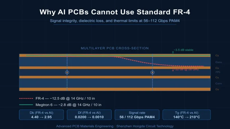
Standard FR-4 laminate — the glass-epoxy workhorse of the PCB industry for over five decades — exhibits Df values in the range of 0.018 to 0.025 at 10 GHz. At 1G and 10G signaling rates, this loss was acceptable. At 112G PAM4, a Df of 0.020 produces approximately 1.0 dB/inch of dielectric insertion loss at 28 GHz. A server backplane with 24-inch traces loses 24 dB to dielectric absorption alone — before accounting for conductor loss, via discontinuities, or connector transitions. The link is inoperable before equalization is even applied.
Ultra-low-loss laminates such as Panasonic Megtron 7, Isola I-Tera MT40, and Park/Nelco NE-9FG achieve Df values between 0.001 and 0.004 at 10 GHz. This ten-fold reduction in Df reduces dielectric insertion loss proportionally, restoring the channel budget that modern modulation schemes require.
Df is not a fixed material property — it rises with temperature and with frequency, at rates that vary significantly between material families. Hydrocarbon-ceramic laminates show the flattest Df versus frequency curves. Modified epoxy and polyphenylene ether (PPE) blends occupy the middle tier. Standard woven-glass epoxies show the steepest frequency dependence. Engineers specifying materials for 112G PAM4 should verify Df values at the application frequency (28 GHz), not at the common 1 GHz or 10 GHz characterization frequencies used in many supplier data sheets.
High-Speed Multilayer PCB Dielectric Material Families: A 2026 Landscape
The table below summarizes the four principal material grades encountered in high-speed multilayer PCB manufacturing, with representative Dk and Df values at 10 GHz, primary application domains, relative cost multipliers, and manufacturing complexity. These values represent industry-typical ranges; specific values should always be confirmed with the laminate manufacturer’s latest data sheets at the operating frequency.
| Material Grade | Typical Dk (10 GHz) | Typical Df (10 GHz) | Best Application | Relative Cost | Mfg Complexity |
| Standard FR-4 | 4.2 – 4.8 | 0.018 – 0.025 | PCIe Gen 1/2, legacy | 1× | Low |
| Mid-Loss (e.g. Isola 370HR) | 3.9 – 4.2 | 0.010 – 0.018 | PCIe Gen 3/4, 25G | 2–3× | Medium |
| Low-Loss (e.g. Megtron 6) | 3.4 – 3.7 | 0.004 – 0.009 | PCIe Gen 5, 56G NRZ | 4–6× | Medium-High |
| Ultra-Low-Loss (e.g. Megtron 7, Rogers 4350B) | 3.0 – 3.5 | 0.001 – 0.004 | 112G PAM4, 800G AI fabric | 8–12× | High |
1. Standard FR-4: Why It Cannot Support 112G PAM4 or PCIe Gen 5
FR-4 remains the dominant PCB laminate globally by volume and will continue to serve the vast majority of cost-sensitive applications — consumer electronics, power supplies, low-speed industrial control. Its limitations at high frequency are not a defect; they are a consequence of the chemistry that makes it affordable. The woven glass reinforcement introduces a periodic inhomogeneity in Dk (sometimes called fiber weave effect) that causes differential-pair skew. The epoxy resin contributes high Df. Neither characteristic can be engineered away while maintaining the price point that has made FR-4 ubiquitous.
For any serial link running at 56 Gbps or above per lane — which covers all 112G PAM4 and PCIe Gen 5 applications — standard FR-4 should be excluded from material consideration at the beginning of the design process, not after signal integrity simulation reveals the loss deficit.
2. Mid-Loss Laminates: The PCIe Gen 4 Workhorse
Materials such as Isola 370HR, Ventec VT-47, and TUC TU-872 SLK occupy the mid-loss tier, with Df values of 0.010 to 0.018 at 10 GHz. They are manufactured on conventional FR-4 production equipment, making them accessible to a broad range of PCB fabricators, including Shenzhen Hongda Circuit Technology Co., Ltd., which processes these materials on standard multilayer lamination lines with tightly controlled bond cycles. Dk stability and Df consistency are markedly better than standard FR-4, and these materials reliably support PCIe Gen 3 and Gen 4 channels at the board lengths typical in server motherboards.
Mid-loss laminates represent a reasonable choice for PCIe Gen 5 only when channel lengths are short (under 150 mm), the operating temperature range is controlled, and active retimers are in the signal path. For Gen 5 backplanes or GPU carrier boards without retimers, the low-loss tier is the minimum practical choice.
3. Low-Loss Laminates: The PCIe Gen 5 and 56G Baseline
The low-loss family — typified by Panasonic Megtron 6, Isola FR408HR, and Ventec VT-901 — achieves Df in the range of 0.004 to 0.009 at 10 GHz through reformulated resin systems that reduce polar molecular groups. These materials are now the production baseline for PCIe Gen 5 servers, 400G switch ASICs, and 56G NRZ infrastructure at Shenzhen Hongda Circuit Technology Co., Ltd. They require more precise lamination control than mid-loss materials — longer cure cycles, tighter temperature uniformity across the press platen, and careful prepreg selection to maintain Dk consistency — but they are established, repeatable processes in any advanced multilayer PCB shop.
4. Ultra-Low-Loss Laminates: Enabling 112G PAM4 and 800G AI Fabric
Ultra-low-loss materials — Panasonic Megtron 7, Isola I-Tera MT40, Rogers 4350B, and Park Nelco NE-9FG among the most widely specified — achieve Df values at or below 0.003 at 10 GHz. Most are built on hydrocarbon or modified PTFE resin systems, sometimes with hollow glass microsphere reinforcement rather than woven fabric to eliminate fiber weave effect. These laminates are now the production standard for 112G PAM4 switch fabrics in hyperscale data centers, 800G CFP8 transceiver PCBs, AI training cluster interconnects, and 5G mmWave base station hardware.
Fabricating ultra-low-loss multilayer PCBs imposes real constraints on the manufacturing process. Resin systems with very low Df are often more chemically resistant, which complicates via drilling, desmear, and copper plating adhesion. Thermal expansion coefficients differ from FR-4, requiring adjusted lamination profiles. At Shenzhen Hongda Circuit Technology Co., Ltd., we have developed qualification protocols for Megtron 7 and I-Tera MT40 that include controlled-atmosphere storage, lamination temperature profiling by panel zone, and 100% impedance verification on coupon arrays using time-domain reflectometry (TDR) before any production panel ships.
Stack-Up Architecture for High-Speed Multilayer PCBs: Material Assignment Strategies
1.Layer-by-Layer Material Assignment in a High-Speed Multilayer PCB
Not every layer in a multilayer PCB carries high-speed differential pairs. A 16-layer AI server motherboard might route 112G PAM4 lanes only on layers 1–2 and 15–16, with the remaining twelve layers devoted to power distribution, USB, I2C, and other sub-1G signals. Paying ultra-low-loss material prices for all sixteen layers adds cost without adding performance.
The standard approach is to assign material grade by electromagnetic field exposure:
| Layer | Function | Recommended Material | Thickness (mm) |
| L1 (Top) | High-speed signal | Ultra-low-loss prepreg | 0.10 – 0.12 |
| L2 | GND reference | Low-loss core | 0.10 |
| L3–L4 | PDN / VRM | Mid-loss core acceptable | 0.20 – 0.30 |
| L5 | GND reference | Low-loss core | 0.10 |
| L6 (Bottom) | High-speed signal | Ultra-low-loss prepreg | 0.10 – 0.12 |
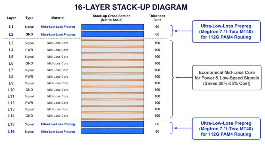
2. Hybrid Stack-Up Design for 112G PAM4 Multilayer PCBs
A hybrid stack-up pairs ultra-low-loss prepregs in the regions adjacent to high-speed signal layers with standard low-loss or mid-loss cores in the interior PDN region. The electromagnetic field of a tightly coupled differential pair is concentrated within approximately two trace widths on either side of the trace — roughly 0.2–0.4 mm for a 100 Ω differential pair on 100 μm dielectric. The core material 1 mm away from the trace contributes negligibly to the dielectric loss seen by the signal.
Hybrid stack-ups are now standard practice at Shenzhen Hongda Circuit Technology Co., Ltd. for multilayer PCBs above 10 layers. The prepreg layers adjacent to L1, L2, L(n-1), and Ln are specified as ultra-low-loss material; the core and prepreg in the interior stack are specified one tier lower. This approach typically reduces total laminate cost by 20–35% compared to a homogeneous ultra-low-loss build while preserving insertion loss performance within 0.3 dB/m of the all-premium-material equivalent.
3. Via Structure and Stub Management in High-Speed Multilayer PCBs
Advanced via architecture and sequential lamination capabilities supporting IPC Class 3 precision at Shenzhen Hongda Circuit Technology Co., Ltd
Via transitions introduce impedance discontinuities and resonance stubs that degrade high-frequency signal quality independently of laminate choice. For 112G PAM4 design on an 8-layer stack-up, backdrilling (controlled-depth drilling to remove unused via barrel) or via-in-pad with resin fill reduces stub length and associated notch losses. In 2026, laser-drilled blind via structures on ultra-low-loss laminates have become the preferred architecture for layer transitions on critical 112G PAM4 channels, eliminating the stub problem at the cost of additional drilling operations.
Shenzhen Hongda Circuit Technology Co., Ltd. offers controlled-depth backdrilling to ±0.1 mm accuracy, laser-drilled blind microvias to IPC-6012 Class 3 on all qualified ultra-low-loss laminates, and sequential lamination for any-layer HDI structures required by advanced 112G PAM4 routing architectures.
Material Selection Framework for 112G PAM4 and PCIe Gen 5 Multilayer PCB Design
1. Channel-Length-Based Material Grade Selection
The choice of dielectric material grade should begin with the channel insertion loss budget, not with cost or supplier preference. A simple decision framework based on channel length and target data rate provides an initial material filter:
- Channels under 100 mm at PCIe Gen 5 (32 GT/s): mid-loss laminates are borderline acceptable with active equalization; low-loss preferred for production yield margin.
- Channels 100–300 mm at PCIe Gen 5: low-loss laminates required; ultra-low-loss recommended for channels above 250 mm or operating above 70 °C.
- Channels under 150 mm at 112G PAM4 (56 GBd): low-loss laminates with optimized copper surface profile.
- Channels 150–400 mm at 112G PAM4: ultra-low-loss laminates required; hybrid stack-up with VLP copper foil recommended.
- Channels over 400 mm at 112G PAM4: ultra-low-loss laminate plus active retimer at mid-channel; evaluate linear retimer versus DSP-based retimer based on power budget.
2. The Role of Copper Foil Profile in High-Speed Multilayer PCB Loss Optimization
Dielectric Df selection is necessary but not sufficient for 112G PAM4 channel optimization. Copper foil surface roughness — quantified by the root-mean-square (RMS) roughness parameter Rq or the ten-point mean roughness Rz — adds resistive loss that is especially significant at frequencies above 10 GHz. Standard electrodeposited (ED) foil exhibits Rz values of 5–8 μm on the bond (rough) side. VLP foil is specified below 2 μm Rz; reverse-treated foil (RTF) achieves 1–3 μm Rz with controlled bonding chemistry.
At 28 GHz, surface roughness loss from standard ED foil can add 0.5–1.0 dB/inch to conductor loss — an amount comparable to the dielectric savings from upgrading from mid-loss to low-loss laminate. Specifying ultra-low-loss dielectric while retaining standard ED copper is a common and expensive design mistake. For 112G PAM4 channels, VLP or RTF copper foil should always accompany ultra-low-loss laminate selection.
3. Temperature, Frequency, and Moisture: Understanding Real-World Df Behavior
Laminate Df values published in data sheets are typically measured at room temperature (23 °C), at a single frequency (often 1 GHz or 10 GHz), on a dry-conditioned specimen. Production PCBs live at elevated temperature under power, and they absorb moisture in humid environments. Both conditions increase Df above the data-sheet value.
In hyperscale data centers, board temperatures of 55–75 °C at the substrate surface are common under sustained load. PPE-based laminates (Megtron 6 family) show Df increases of approximately 10–15% from 25 °C to 75 °C. PTFE-based laminates (Rogers 4350B) show increases below 5% over the same range, making them preferable for thermally stressed 112G PAM4 applications despite higher fabrication complexity.
Moisture absorption above 0.5% by weight is sufficient to measurably increase Df in most resin systems. Multilayer PCBs for outdoor 5G base station hardware or automotive ADAS modules should be evaluated with moisture-conditioned specimens using IPC-TM-650 2.5.5.7 or equivalent protocols before material finalization.
2026 Advances in PCB Dielectric Materials for High-Speed Multilayer Design
The laminate material landscape has advanced substantially in the two years leading to 2026, driven by demand from AI accelerator platforms, 800G optical transport, and automotive ADAS programs.
1. Next-Generation Ultra-Low-Loss Laminates Entering Volume Production in 2026
Panasonic’s Megtron 7 NX variant, released for volume production in early 2025, achieves a Df of 0.0015 at 10 GHz with improved dimensional stability versus the original Megtron 7. This material has been qualified for 224G PAM4 channel evaluation — the architecture being standardized under IEEE 802.3dj — and is beginning to appear in 112G PAM4 production designs where it provides margin that enables longer channels or relaxed equalization requirements.
Isola’s I-Tera MT40+ extends the original I-Tera MT40 formulation with a modified glass weave that reduces fiber weave effect by approximately 40% compared to standard 1078 glass styles. This is significant for differential pair skew on long routes, where conventional low-profile glass weaves introduce measurable common-mode noise through differential Dk variation between the two conductors of a pair.
Rogers Corporation has extended the 4000 series with the 4835HT, targeting mmWave PCB applications above 77 GHz for automotive radar and 5G FR2. While not directly relevant to 112G PAM4 (which remains below 56 GHz), the processing improvements in high-frequency PTFE-ceramic systems have cross-pollinated into the lower-frequency ultra-low-loss product lines.
2. AI-Driven Process Optimization in High-Speed Multilayer PCB Fabrication
2025 and 2026 have seen widespread adoption of machine-learning-based process control in advanced PCB fabrication. At Shenzhen Hongda Circuit Technology Co., Ltd., real-time dielectric thickness measurement using terahertz time-domain spectroscopy (THz-TDS) is integrated with our lamination press control systems, enabling closed-loop Dk uniformity control to ±0.05 across the panel — a specification that was achievable only in aerospace-grade fabrication environments as recently as 2023.
AI-assisted via drilling path optimization now accounts for substrate fiber weave orientation when scheduling controlled-depth backdrilling, reducing stub-length variation by 30–40% compared to conventional drilling sequences. This improvement is significant because stub resonance frequency variation is a leading cause of yield loss on high-speed multilayer PCBs at the final electrical test stage.
3. Embedded Components in High-Speed Multilayer PCBs: 2026 Maturation
Embedded passive technology — particularly embedded capacitors for PCIe Gen 5 and AI accelerator power delivery — has reached production maturity in 2025–2026. Embedded capacitance layers using high-Dk, high-Df materials are isolated from signal layers by ultra-low-loss prepreg, allowing the power distribution network to benefit from intimate decoupling capacitance without contaminating the signal channel with lossy dielectric. This architecture is now available in Shenzhen Hongda Circuit Technology Co., Ltd.’s advanced multilayer PCB product line for configurations up to 20 layers.
Shenzhen Hongda Circuit Technology Co., Ltd.: High-Speed Multilayer PCB Manufacturing Capabilities
Shenzhen Hongda Circuit Technology Co., Ltd. brings more than two decades of advanced multilayer PCB fabrication experience to high-speed dielectric material processing. Our technical capabilities specific to 112G PAM4 and PCIe Gen 5 applications include:
- Qualified laminate portfolio: Full qualification on Megtron 6, Megtron 7, I-Tera MT40, FR408HR, and Rogers 4350B, with incoming material acceptance testing that verifies Dk and Df against supplier specifications at 10 GHz using split-post dielectric resonator measurement.
- Controlled impedance manufacturing: 50 Ω single-ended and 100 Ω differential impedance held to ±5% tolerance on all high-speed multilayer PCBs, verified by TDR on production coupons per IPC-2141B.
- Via fabrication: Laser-drilled blind microvias from 75 μm diameter, controlled-depth backdrilling to ±0.1 mm, and via-in-pad with resin fill on all qualified ultra-low-loss laminate systems.
- Layer count and complexity: Up to 32 layers in sequential lamination for HDI structures, with any-layer interconnect capability on 2026-qualified Megtron 7 stack-ups.
- Copper foil options: Standard ED, VLP (<2 μm Rz), and RTF copper foil available on all laminate families, with foil-laminate adhesion qualification per IPC-TM-650 2.4.8.
- Quality and reliability: IPC Class 3 fabrication, ISO 9001:2015, IATF 16949 for automotive applications, and ITAR-compliant production areas for defense programs.
- Design for Manufacturing support: Pre-production DFM review with signal integrity correlation between customer simulation models and fabricated coupons, enabling material and stack-up iteration before first-article production.
Our engineering team collaborates directly with hardware design teams to translate signal integrity simulation targets — insertion loss masks, return loss requirements, differential skew limits — into manufacturing specifications, laminate selections, and stack-up architectures that are achievable in volume production.
Practical Material Selection Checklist for 112G PAM4 and PCIe Gen 5 Multilayer PCB Projects
Design teams approaching a new high-speed multilayer PCB project should validate the following decisions before committing to a laminate:
- Define the channel loss budget: calculate available insertion loss at Nyquist frequency for every trace length in the design. Use the specification worst-case channel model, not the typical case.
- Verify Df at the operating frequency, not at 1 GHz or 10 GHz. Request supplier data at 28 GHz for 112G PAM4 and at 16 GHz for PCIe Gen 5.
- Account for temperature derating: add 15–20% to Df if junction temperature at the PCB surface exceeds 50 °C during normal operation.
- Match copper foil surface profile to laminate grade: always specify VLP or RTF foil alongside ultra-low-loss dielectric for 112G PAM4 applications.
- Validate fiber weave orientation for differential pairs: align trace angle to 0° or 45° relative to glass weave direction, or specify a spread-weave or quasi-isotropic glass style.
- Perform hybrid stack-up analysis: determine which layers carry high-speed signals, and apply premium material only to those dielectric layers within the field distribution of the trace.
- Engage the PCB fabricator early: laminate availability, minimum order quantities, and process qualifications vary by facility. Shenzhen Hongda Circuit Technology Co., Ltd. recommends design review at the stack-up definition stage, before schematic capture is complete.
- Run thermal simulation alongside signal integrity simulation: dielectric Df is a function of temperature, and a board that passes SI simulation at 25 °C may fail at 85 °C operating temperature if material thermal behavior is not modeled.
Dielectric Material Selection as the Foundation of 112G PAM4 and PCIe Gen 5 Signal Integrity
The signal integrity performance of any 112G PAM4 or PCIe Gen 5 high-speed multilayer PCB is ultimately bounded by the dielectric material from which it is built. No equalization architecture, no FEC scheme, and no retimer topology can recover a channel whose physical loss exceeds the receiver’s equalization capability — and at 28 GHz and above, an incorrect laminate choice consumes that capability before the signal reaches its first connector.
The engineering principles governing dielectric selection are clear: Df is the dominant loss parameter at high frequency, it must be evaluated at the operating frequency rather than the characterization frequency, and it degrades with temperature and moisture in ways that must be budgeted into the channel model. Ultra-low-loss laminates with VLP copper foil are the practical engineering requirement for 112G PAM4 channels above 150 mm; low-loss laminates cover PCIe Gen 5 in the channel lengths typical of server motherboards.
2026 has brought meaningful advances in laminate chemistry — lower Df variants of established ultra-low-loss product families, improved fiber-weave constructions that reduce differential skew, and AI-assisted fabrication process control that translates material properties into manufactured performance with new consistency. These advances extend the viable channel reach of 112G PAM4 interconnects and provide the margin headroom that 224G PAM4 standardization will require.
Shenzhen Hongda Circuit Technology Co., Ltd. is qualified and production-ready on the full spectrum of high-speed multilayer PCB laminate materials discussed in this paper. Our engineering team is available to support laminate selection, hybrid stack-up design, signal integrity correlation, and volume manufacturing for 112G PAM4, PCIe Gen 5, 800G, and next-generation AI accelerator platform programs.
FAQ
Which PCB materials are required for PCIe Gen 5 and 112G PAM4 applications?
For PCIe Gen 5 and 112G PAM4 signaling, standard FR-4 laminates are completely excluded due to excessive insertion loss and fiber weave effects. For standard PCIe Gen 5 server motherboards with typical channel lengths, Low-Loss materials like Panasonic Megtron 6, Isola FR408HR, or Ventec VT-901 serve as the production baseline. For critical 112G PAM4 AI server networks, hyperscale switch fabrics, and 800G optical modules, Ultra-Low-Loss laminates such as Megtron 7, Isola I-Tera MT40, or Rogers 4350B are mandatory to maintain the link budget. At Shenzhen Hongda Circuit Technology Co., Ltd., we maintain full qualification and raw material stock across all these high-speed dielectric tiers.
How can I reduce the material cost of a high-speed multilayer PCB?
The most effective manufacturing strategy to optimize budget is using a Hybrid Stack-up design. Not every layer in a 12-layer or 16-layer AI server board carries critical 112G ultra-high-speed signals. At Shenzhen Hongda Circuit Technology Co., Ltd., we recommend deploying premium ultra-low-loss prepregs only on the specific layers adjacent to high-speed lines, while utilizing more economical mid-loss or standard low-loss cores in the interior power-distribution network (PDN) zones. This engineering approach typically reduces total laminate raw material costs by 20% to 35% while preserving over 95% of signal integrity performance.
Why do I need to specify VLP or RTF copper foil alongside low-loss dielectrics?
Specifying an expensive ultra-low-loss laminate while retaining standard Electrodeposited (ED) copper is a very common and costly procurement mistake. At high frequencies like 28 GHz (Nyquist for 112G PAM4), signal currents crowd to the very edge of the copper due to the skin effect. Standard ED copper has a rough surface (5–8 $\mu$m $R_z$) that acts as a longer resistive path, adding significant conductor loss and negating the savings of buying low-loss resin. For high-speed applications, you must match your dielectric with Very-Low-Profile (VLP, <2 $\mu$m $R_z$) or Reverse-Treated (RTF, 1–3 $\mu$m $R_z$) copper foils. Shenzhen Hongda Circuit provides both foil types across all qualified high-speed material families.
What are your impedance control and testing standards for high-layer count high-speed PCBs?
At Shenzhen Hongda Circuit Technology Co., Ltd., we hold controlled single-ended (50 $\Omega$) and differential (100 $\Omega$) impedances to a tight $\pm$5% or $\pm$10% tolerance class, fully compliant with IPC-2141B standards. We do not rely on guesswork; 100% of our production panels are verified using Time-Domain Reflectometry (TDR) on test coupons prior to shipment. Furthermore, for 2026-generation ultra-HDI layouts, we utilize cutting-edge terahertz time-domain spectroscopy (THz-TDS) integrated within our lamination systems to ensure real-time closed-loop dielectric thickness uniformity across every single panel zone.
What manufacturing capabilities do you offer for layer transitions and via structures in 112G PAM4 designs?
To eliminate the resonance stubs that degrade high-frequency performance, Shenzhen Hongda Circuit offers a comprehensive suite of advanced via processing. Our facilities are equipped for highly precise controlled-depth backdrilling to a $\pm$0.1 mm tolerance accuracy, ensuring the removal of unused via barrels on high-speed traces. For ultra-dense packaging or any-layer HDI requirements, we provide laser-drilled blind and buried microvias starting at 75 $\mu$m diameters with resin fill and capping per IPC-6012 Class 3 specifications, providing perfect routing yields for fine-pitch BGA breakouts.
About Author
David Chen https://www.linkedin.com/in/pcbcoming
David Chen boasts an extensive professional background in PCBA manufacturing, PCBA testing, and PCBA optimization, with specialized expertise in high-precision PCBA fault analysis and rigorous PCBA reliability testing. The author has worked with high-layer-count server PCB fabrication, ultra-low-loss backplane stackups, and thermo-mechanical reliability optimization for AI infrastructure projects involving 112G and 224G PAM4 architectures. Skilled in complex circuit design and cutting-edge advanced PCB manufacturing processes, he delivers solutions that elevate product durability and performance across industrial applications. His technical articles focusing on PCBA manufacturing workflows and testing methodologies are widely cited by industry peers, research institutions, and technical platforms, solidifying his reputation as a recognized technical authority in the global circuit board manufacturing sector.