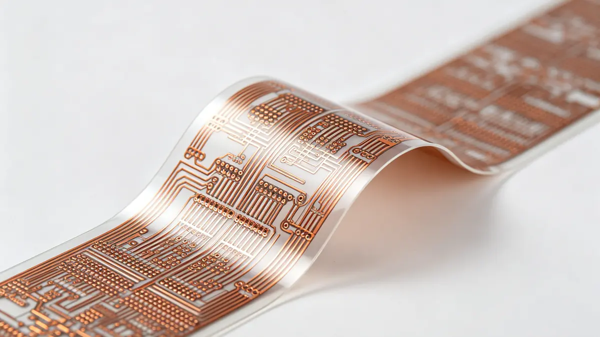
What are the key design constraints for ultra-thin flexible HDI PCBs in smart bands (thickness, bending cycles, impedance control)?
This article outlines 2026 design constraints of ultra-thin flexible HDI PCBs for smart bands, covering thickness limits, bending cycle standards and impedance tolerance, plus latest manufacturing processes and verified industry data.
What is the maximum total thickness for ultra-thin flexible HDI PCBs in smart bands (2026 manufacturing)?
Answer: The maximum total thickness is 0.2 mm, with typical stack-ups at 0.1–0.15 mm.
- Single‑layer flex (12 μm Cu + 25 μm PI + 25 μm coverlay): 0.062 mm
- 2‑layer HDI (1+N+1) with no‑adhesive PI: 0.12–0.15 mm
- 4‑layer rigid‑flex (flex section): ≤0.2 mm
- Dielectric core thickness: 25–50 μm (high‑frequency LCP/PI)
- 2026 process: Vacuum lamination + laser microvia (≤50 μm) enables 0.2 mm HDI with 6 layers
What are the minimum bending cycle requirements for smart band flexible HDI PCBs (dynamic bending, 2026)?
Answer: Minimum 100,000 dynamic bending cycles at 3 mm radius, 180° bend.
- 2026 baseline (RA copper + no‑adhesive PI): ≥100,000 cycles
- Premium grade (Dupont Kapton FN + rolled Cu): 150,000–200,000 cycles
- Bend radius constraint: Dynamic ≥3 mm (12× total thickness); static ≥1 mm
- Trace rule: Route perpendicular to bend axis to avoid cracking
- 2026 material upgrade: New PI blends boost bend life by 30% vs 2024
What impedance control accuracy is required for smart band HDI PCBs (50Ω/100Ω, 2026)?
Answer: ±5% tolerance for 50Ω single‑ended and 100Ω differential pairs.
- 50Ω (BLE/2.4 GHz): ±5% (47.5–52.5Ω)
- 100Ω differential (sensor signals): ±5% (95–105Ω)
- Line width/space: 30/30 μm (2026 LDI process)
- Dielectric constant (Dk): 3.5±0.2 (PI) or 3.0±0.1 (LCP) at 1 GHz
- 2026 method: Laser direct imaging + FEA simulation → impedance error <3%
What 2026 advanced manufacturing technologies enable ultra‑thin flexible HDI for smart bands?
Answer: Key 2026 tech: no‑adhesive PI, laser microvia, LDI, vacuum lamination, and embedded trace.
- No‑adhesive PI substrate: 25–38 μm, Tg>250°C, Df≤0.007@1 GHz; eliminates glue creep, enables 0.1 mm thickness
- UV laser microvia (2026): 30–50 μm diameter, 1:1 aspect ratio; replaces 100 μm mechanical holes, saves 40% space
- Laser Direct Imaging (LDI): 15/15 μm line/space (mass production); ±2 μm accuracy, supports 0402/0201 components
- Vacuum sequential lamination: ≤0.75% warpage (2026 control); 0.1 μm layer alignment, prevents delamination in 0.2 mm stacks
- Rolled Annealed (RA) copper: 12–18 μm, elongation >20% (vs 8–12% electroplated); bend life 2× longer
What are the key material constraints for 2026 ultra‑thin flexible HDI in smart bands?
Answer: Materials must balance low loss, high bend life, and ultra‑thin form factors.
- Substrate: Polyimide (PI) (Dk=3.5–3.8, Tg>250°C) or LCP (Dk=3.0, Df<0.003)
- Copper: RA copper (12 μm/0.5oz standard); tensile strength ≥300 MPa
- Coverlay: 25 μm PI, laser‑cut openings; peel strength >1.2 N/mm
- Adhesive: No‑adhesive construction preferred (2026); reduces thickness by 20–30 μm
- Thermal stability: withstand −40°C to 125°C; 260°C reflow compatible
FAQ
Q1: Can a smart band flexible HDI PCB be thinner than 0.1 mm in 2026?
A1: Yes—single‑layer no‑adhesive PI can reach 0.05–0.06 mm; multi‑layer HDI minimum 0.1 mm.
Q2: What is the maximum layer count for 0.2 mm flexible HDI in smart bands?
A2: Up to 6 layers (2+2+2) with laser microvias and sequential lamination (2026).
Q3: How to maintain impedance control when bending?
A3: Use LCP dielectric (stable Dk under flex), route traces perpendicular to bend axis, and fix coverlay thickness at 25 μm.
Still, need help? Contact Us: sales@pcbkr.com
Need a PCB or PCBA quote? Quote now
About Author
David Chen https://www.linkedin.com/in/pcbcoming/
David Chen boasts an extensive professional background in PCBA manufacturing, PCBA testing, and PCBA optimization, with specialized expertise in high-precision PCBA fault analysis and rigorous PCBA reliability testing. Skilled in complex circuit design and cutting-edge advanced PCB manufacturing processes, he delivers solutions that elevate product durability and performance across industrial applications. His technical articles focusing on PCBA manufacturing workflows and testing methodologies are widely cited by industry peers, research institutions, and technical platforms, solidifying his reputation as a recognized technical authority in the global circuit board manufacturing sector.