What is the biggest pain point in high-frequency PCB manufacturing?
Key Pain Points in High-Frequency PCB Manufacturing (Engineering Perspective)
For senior engineers, the biggest challenges in manufacturing high-frequency PCBs can be summarized as “three highs and one low”: difficult-to-process materials, extremely tight impedance control, hard-to-reduce signal loss, and an uneasy balance between yield and cost. A tolerance deviation in any step can lead to signal failure.
Four Core Pain Points
1. Extremely Difficult Processing of High-Frequency Materials
High-frequency boards typically use PTFE, ceramic-filled, or hydrocarbon substrates (e.g., Rogers), which behave very differently from standard FR-4:
- PTFE is soft (Shore 50D), causing burrs, rough hole walls, and shrinkage during drilling; edge milling easily leads to chipping; handling causes deformation, resulting in very low process efficiency.
- Ceramic and hydrocarbon substrates are hard and brittle, leading to rapid drill bit wear (standard bits fail after 200 holes), with tooling costs 3–5 times higher than for standard boards.
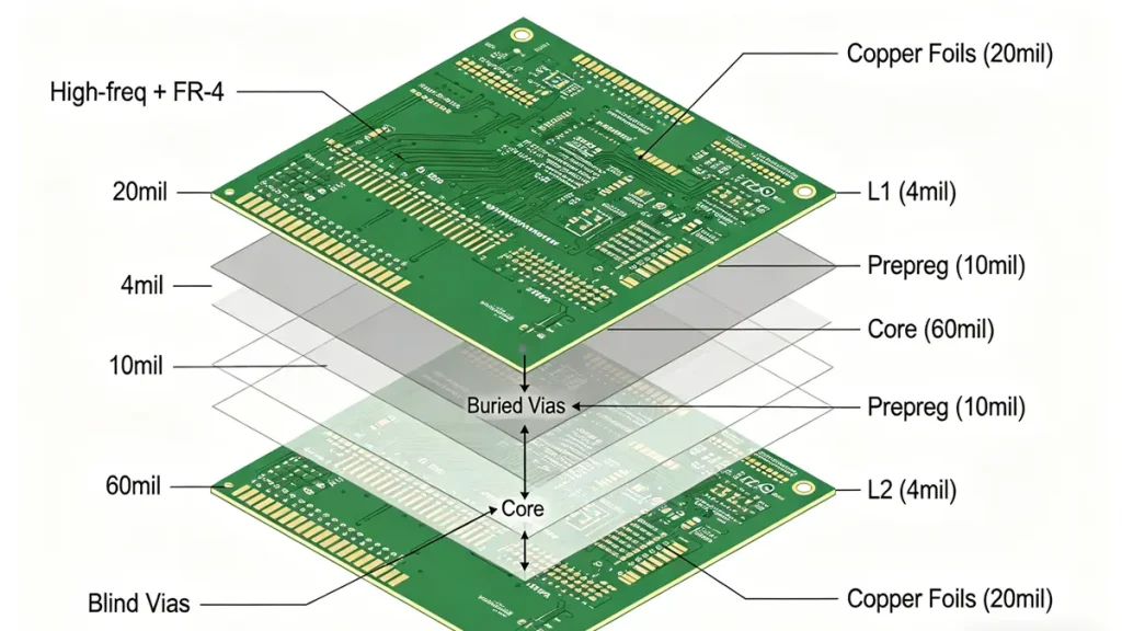
- Imported laminates have limited inventory and long lead times. Hybrid stacking (high-frequency + FR-4) creates difficulties in controlling resin flow and coefficient of thermal expansion (CTE), with an extremely narrow lamination process window.
2. Stringent Impedance Control with Minimal Tolerance
High-frequency signals are highly sensitive to impedance, requiring tolerance within ±5% (±3% for ultra-high speed), far tighter than the ±10% for standard PCBs:
- Batch variations in material Dk/Df, uneven lamination thickness, etching width deviation, and plating thickness variation can all push impedance out of spec.
- Vias and pads break impedance continuity; stacked or blind vias increase equivalent capacitance and cause reflections; residual stub length from back drilling severely degrades high-frequency performance.
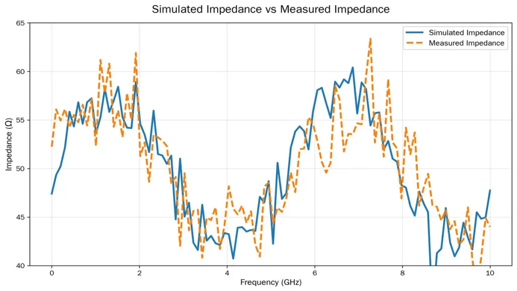
- Disconnection between design and manufacturing: theoretical simulation often mismatches real process conditions (e.g., copper roughness, actual dielectric thickness), leading to inconsistent impedance between prototyping and mass production.
3. Sharply Rising Insertion Loss Prone to Closed Eye Diagrams
At speeds above 10 Gbps, insertion loss directly determines transmission quality:
- Dielectric loss: Molecular polarization lag at high frequencies converts signal energy into heat; higher Df increases loss.
- Conductor loss: Skin effect concentrates current on the copper surface; micro-roughness raises effective resistance, increasing loss by up to 15% above 10 GHz.
- Extremely high routing density (line/space ≤40 μm) intensifies crosstalk and significantly increases EMI radiation risk.
4. Conflict Between Heat Dissipation and Reliability
Most high-frequency materials have poor thermal conductivity, while high-speed chips generate considerable heat. Heat buildup causes Dk drift, degrading signal stability or even causing device failure.
- Multilayer HDI boards (20+ layers) suffer from accumulated registration errors due to lamination stress release, with high risk of misalignment between blind vias and inner-layer circuits.
- Surface finish thickness (ENIG, immersion silver) slightly adjusts final impedance, requiring delicate trade‑offs between reliability and impedance control.
Summary and Mitigation Strategies
High-frequency PCB manufacturing demands precise coordination across materials, design, processing, and testing. The core pain points are the conflict between processability and electrical performance, extreme requirements for impedance and loss, and balancing batch stability with cost.
Key mitigations:
- Materials: Select high-frequency substrates with stable Dk/Df and good batch consistency (e.g., Rogers 4350B); carefully evaluate CTE and resin flow for hybrid stacks.
- Processes: Use laser drilling (hole diameter ±15 μm), very low-profile (VLP) copper foil, and plasma activation for PTFE hole walls; tightly control etching undercut and lamination tolerances.
- Design‑manufacturing collaboration: Early CAM review and impedance simulation; clearly define tolerances for line width, dielectric thickness, and copper weight to ensure design for manufacturability (DFM).
High-Frequency PCB Engineering Guide
Ready-to-Use: Process Parameters, Material Selection & Pain Point Solutions
(Factory-proven for mass production, prototyping & export; directly actionable for PCB manufacturers)
I. Core Pain Point (One-Sentence Summary)
High-frequency PCBs follow a brutal rule: Higher performance = harder to manufacture; tighter impedance = more loss-sensitive; costlier materials = lower yield.
All issues boil down to five critical factors:
Dk stability, copper roughness, dielectric thickness, linewidth tolerance, via stub length.
II. Material Selection (Factory-Approved)
1. Frequency-Matched Materials (No Failures)
- <6 GHz: Standard hydrocarbon systems → Megtron 6/7, TU-872, Isola Astra
- 6–20 GHz: Mid-high frequency → Rogers 4350B, 4003C, Taconic TLY-5
- 20–60 GHz: Millimeter-wave → Rogers 5880, Taconic TLX-8, RO3003
- Hybrid (High‑Freq + FR‑4): Rogers 4350B + S1000‑2M (most stable)
2. Non-Negotiable Key Parameters
- Dk tolerance: ≤±0.05 (otherwise impedance drifts severely)
- Df: ≤0.003 (higher Df = higher loss)
- Copper foil: HVLP/RTF ultra‑low profile (roughness Rz <1 μm)
- Standard copper: Rz ≈3–5 μm, increases high-frequency loss by 20%+
III. Impedance Control (Make-or-Break for High-Freq)
Mandatory Tolerances (Spec Required)
- Standard PCB: ±10%
- High‑freq / high‑speed: ±5% (required)
- 112G / PCIe 5.0 / mmWave: ±3%
Top 3 Impact Factors
- Dielectric thickness tolerance: within ±10%
- Linewidth tolerance: ±0.02 mm (20 μm)
- Copper weight: prefer 1/3 oz (12 μm); 1 oz NOT recommended
IV. Insertion Loss (Top Engineer Headache)
Three Major Loss Sources
- Conductor loss (skin effect)→ Must use low‑profile HVLP copper
- Dielectric loss→ Minimize Df; standard FR‑4 is NOT suitable for high frequency
- Roughness loss→ Rougher copper = higher loss
Rule of thumb: At 10 GHz, standard copper has 15–25% higher loss than HVLP.
V. Vias & Back Drilling (Hidden Killer)
Pain point: Via stubs cause signal reflection and collapsed eye diagrams.
Mandatory Requirements
- Back-drilled stub: ≤6 mil (0.15 mm)
- Preferred: blind/buried vias + back drilling to minimize stubs
- Minimize via pad size; enlarge anti-pad to reduce parasitic capacitance
VI. Process Control Parameters (Send Directly to PCB Factory)
1. Drilling
- PTFE & high‑freq materials: laser drilling preferred
- Spindle speed: ≥120 krpm
- Slow feed rate to avoid burrs, rough holes, and edge chipping
2. Electroless Copper & Electroplating
- PTFE requires plasma treatment to prevent copper peel-off
- Hole copper thickness: 20–25 μm, uniformity ±2 μm
3. Etching
- Undercut: ≤15 μm
- Linewidth uniformity: ±0.02 mm
4. Lamination
- Multilayer boards: strict pressure & temperature profiling
- Thickness tolerance: within ±10%
- Hybrid stacks: mandatory stress testing to prevent delamination & warpage
5. Surface Finish
- Only recommended for high freq: ENIG (Electroless Nickel Immersion Gold)
- Gold thickness: 0.05–0.1 μm
- Nickel thickness: 3–5 μm
- Prohibited: OSP, HASL, thick gold (all alter impedance)
VII. Standard Configurations by Application (Copy-Paste Ready)
1. 5G Base Station / RF Board (6–20 GHz)
- Material: Rogers 4350B
- Impedance: ±5%
- Copper: HVLP 1/3 oz
- Back drill: stub ≤0.15 mm
- Finish: ENIG
2. High-Speed Digital (PCIe 5.0 / 112G)
- Material: Megtron 7 / Isola Astra
- Impedance: ±3%
- Copper: HVLP
- Back drilling: required
- Strict dielectric thickness control
3. Millimeter-Wave Radar (24–77 GHz)
- Material: RO3003 / 5880
- Impedance: ±3%
- Copper: ultra-smooth foil (Rz <1 μm)
- Minimize vias; use small vias & short stubs
VIII. Top 3 Pain Points From Real High-Freq PCB Engineers
- Better material performance = worse processability & lower yield.
- Impedance simulation looks perfect, but real boards don’t match.
- Vias and stubs are invisible killers—eye diagrams collapse instantly in testing.
Still, need help? Contact Us: sales@pcbkr.com
Need a PCB or PCBA quote? Quote now
About Author
David Chen https://www.linkedin.com/in/pcbcoming/
David Chen boasts an extensive professional background in PCBA manufacturing, PCBA testing, and PCBA optimization, with specialized expertise in high-precision PCBA fault analysis and rigorous PCBA reliability testing. Skilled in complex circuit design and cutting-edge advanced PCB manufacturing processes, he delivers solutions that elevate product durability and performance across industrial applications. His technical articles focusing on PCBA manufacturing workflows and testing methodologies are widely cited by industry peers, research institutions, and technical platforms, solidifying his reputation as a recognized technical authority in the global circuit board manufacturing sector.