High-Speed PCB Solutions
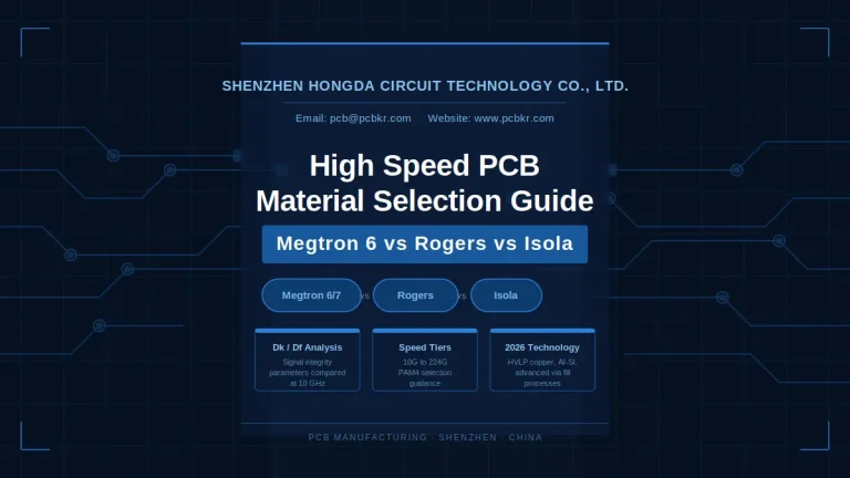
High-Speed PCB: Mastering Impedance & Signal Loss
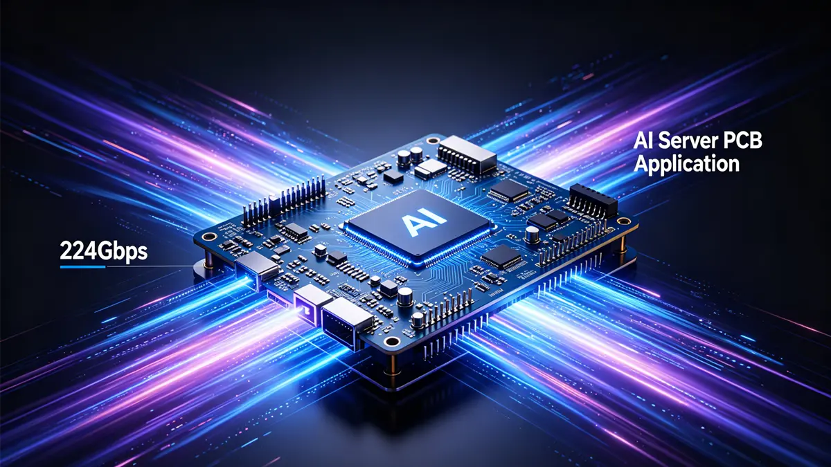
In the era of 224Gbps signal integrity and AI-driven infrastructure, high-frequency PCB manufacturing has evolved into a high-stakes engineering challenge defined by the “three highs and one low”: difficult-to-process materials, extremely tight impedance control, hard-to-reduce signal loss, and the delicate balance between yield and cost.
For senior engineers, understanding these pain points is the first step toward successful mass production. Here is a factory-proven guide to navigating the complexities of high-speed PCB fabrication.
1. The Material Challenge: Beyond Standard FR-4
High-frequency boards demand substrates like PTFE (e.g., Rogers), ceramic-filled, or hydrocarbon systems to maintain electrical performance. However, these materials introduce significant processing hurdles:
- PTFE Softness: With a Shore hardness of 50D, PTFE is prone to deformation, burrs, and rough hole walls during drilling.
- Tooling Costs: Hard ceramic fillers cause rapid drill bit wear—standard bits often fail after just 200 holes—increasing tooling costs by 3–5 times.
- Hybrid Stacking: Combining high-frequency laminates with FR-4 requires precise control over resin flow and Coefficient of Thermal Expansion (CTE) to prevent delamination.+1
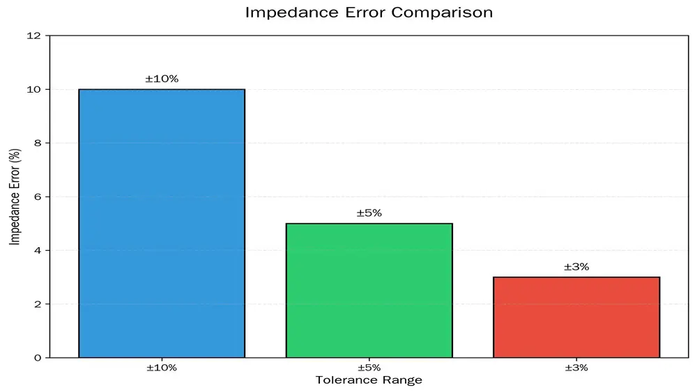
2. Precision Impedance Control: The ±3% Requirement
While standard PCBs allow for a ±10% impedance tolerance, high-speed applications like PCIe 5.0 or 112G demand a much tighter ±5% or even ±3%.+1
- Critical Factors: Variations in dielectric thickness, etching undercut, and copper weight can instantly push a board out of spec.
- Tight Tolerances: Achieving these standards requires linewidth uniformity within ±0.02 mm and dielectric thickness tolerance within ±10%.+1
- The “Stub” Killer: Via stubs act as resonators that collapse eye diagrams; maintaining a back-drilled stub length of ≤6 mil (0.15 mm) is mandatory for signal integrity.+2
3. Combatting Insertion Loss at 10GHz+
As speeds cross the 10 Gbps threshold, insertion loss becomes the primary determinant of transmission quality.
- Conductor Loss & Skin Effect: At high frequencies, current concentrates on the copper surface. Using Very Low Profile (VLP) or HVLP copper foil (roughness Rz<1 \mum) can reduce loss by up to 15%–25% compared to standard copper.+3
- Dielectric Loss: Choosing materials with a stable Df≤0.003 is essential to prevent signal energy from converting into heat.+1
4. Factory-Proven Process Parameters
To ensure reliability and batch stability, we implement the following manufacturing standards:
- Drilling: Laser drilling is preferred for PTFE and HDI structures, with spindle speeds ≥120 krpm to ensure hole wall quality.
- Surface Finish: ENIG (Electroless Nickel Immersion Gold) is the recommended finish, as it provides a flat surface without significantly altering impedance.+1
- Plasma Activation: PTFE hole walls must undergo plasma treatment to ensure proper copper bonding and prevent peeling.
Summary and Mitigation Strategies
High-frequency PCB success requires a “Design for Manufacturability” (DFM) approach. By selecting materials with stable Dk/Df tolerances (≤±0.05), utilizing HVLP copper, and enforcing strict back-drilling stubs, manufacturers can balance high-end performance with cost-effective yields.+4
Need expert guidance on your next High-Frequency project? Contact our engineering team at sales@pcbkr.com for a technical review or a rapid quote.
Tags: #HighFrequencyPCB #ImpedanceControl #SignalIntegrity #PCBMaterial #HighSpeedPCB #PCBManufacturing
Still, need help? Contact Us: sales@pcbkr.com
Need a PCB or PCBA quote? Quote now
About Author
David Chen https://www.linkedin.com/in/pcbcoming/
David Chen boasts an extensive professional background in PCBA manufacturing, PCBA testing, and PCBA optimization, with specialized expertise in high-precision PCBA fault analysis and rigorous PCBA reliability testing. Skilled in complex circuit design and cutting-edge advanced PCB manufacturing processes, he delivers solutions that elevate product durability and performance across industrial applications. His technical articles focusing on PCBA manufacturing workflows and testing methodologies are widely cited by industry peers, research institutions, and technical platforms, solidifying his reputation as a recognized technical authority in the global circuit board manufacturing sector.