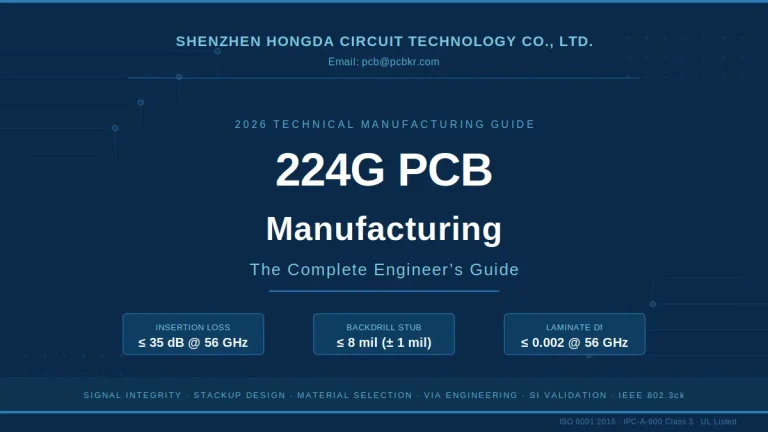
7 Strategies to Shorten Fast-Turn PCB Lead Times in 2026 High-Precision Era
7 Strategies to Shorten Fast-Turn PCB Lead Times in 2026
Published by: Engineering Department, Shenzhen Hongda Circuit Technology Co., Ltd.
Foreword: Evolution from “Speed” to “Predictive Precision”
Entering 2026, the global electronics industry is at a pivotal stage marked by the boom of AI infrastructure (e.g., Nvidia Blackwell and Rubin architectures), large-scale deployment of 1.6T networks, and pre-research for 6G. Against this backdrop, hardware engineers face unprecedented challenges: PCBs are no longer just carriers for components, but sophisticated electromagnetic transmission systems.
At Shenzhen Hongda Circuit Technology Co., Ltd., we have observed a fundamental shift in the traditional concept of “Fast Turn”. In the past, fast turnaround relied on overtime labor; today, with 120-layer ultra-high-density designs and 224Gbps signal rates, speed must be built on predictive precision. Even a minor engineering rework can result in weeks of lost time.
Below are Hongda Circuit’s seven core strategies to shorten lead times through technological innovation in 2026.
1. AI-Driven “Zero-Loop” DFM Intelligent Audit
The biggest time-waster in PCB manufacturing is the back-and-forth of engineering confirmation (EQ) between designers and factories. Traditional DFM checks depend on manual experience, often taking 24–48 hours to provide feedback.
Hongda’s Solution
We have deployed the latest 2026 AI-driven Design for Manufacturability (DFM) system, integrated with our decade-plus database of high-end manufacturing expertise. When customers upload Gerber files, the AI completes an in-depth scan of 120-layer stackups in minutes.
- Intelligent Recognition: Automatically detects residual copper effects, impedance mismatches in 224Gbps high-speed paths, and potential open-circuit risks at 10μm line widths.
- Physical Simulation: Beyond checking clearances, the AI simulates resin flow and filling during lamination to predict voids in high-density areas.
This “zero-loop” model ensures engineering releases to production within 1 hour, eliminating two full days of communication from the traditional workflow.
2. Strategic Stockpiling of 224Gbps-Specific Materials
In 2026, supply chain stability has become the biggest variable for lead times. Especially for M9-grade ultra-low-loss substrates and VLP2 (very low profile) copper foils used in AI servers and 800G/1.6T switches, lead times often stretch 4–6 weeks.
Hongda’s Solution
As a high-end market-focused manufacturer, Hongda Circuit has established a Strategic Material Assurance Warehouse.
- Core Stock: We maintain ready stock of all specifications of ultra-low-loss (ULL) materials, LCP substrates, and high-performance metal-core materials (9.0 W/m·K).
- Skin Effect Control: For sub-THz applications, we stock specialized VLP2 copper foil to effectively suppress high-frequency skin-effect loss.
By reducing “material waiting time” to zero, we offer “next-day launch” ultra-responsive service for high-frequency prototype projects such as ZL Design or RadioMate.
3. Digital Twin Registration Technology for 120-Layer Ultra-High-Density Stackups
Registration difficulty increases exponentially with layer count. For 120-layer ultra-high-density HDI boards, a mere 10μm shift in any layer can scrap the entire panel—and re-producing a 120-layer board typically takes over 15 days.
Hongda’s Solution
We have adopted cutting-edge 2026 Digital Twin Registration systems.
- Dynamic Compensation: The system builds a virtual digital model for each inner layer. Laser Direct Imaging (LDI) equipment adjusts exposure parameters for the next layer in real time based on actual thermal expansion and contraction of each layer during lamination.
- Blind Via Precision: Paired with 5μm laser microvia technology, we ensure precise interconnection of thousands of microvias within 120 layers.
This technology eliminates rework risks and shortens the manufacturing cycle of high-layer-count boards by 40%.
4. mSAP Process: “Rapid Growth” for Fine Circuitry
Traditional subtractive etching struggles with 10μm line/space designs: side etching is hard to control, process chains are long, and yield fluctuates widely.
Hongda’s Solution
We have fully implemented the mSAP (Modified Semi-Additive Process). Unlike the traditional logic of “etching away excess copper”, mSAP “grows” circuitry on an ultra-thin base copper layer.
- Sidewall Verticality: mSAP produces perfectly rectangular conductor cross-sections, critical for signal integrity.
- Efficiency Boost: The process reduces time uncertainty caused by multiple chemical etching steps.
For medical devices or 6G modules requiring extreme miniaturization, mSAP cuts turnaround time by 25% compared to traditional HDI while maintaining precision.
5. AI Real-Time Impedance Compensation: Defending the ±5% Tolerance Limit
For 224Gbps high-speed transmission, tightening impedance tolerance from ±10% to ±5% is mandatory. Traditional manufacturing often detects impedance failures only after final testing, resulting in scrapped boards.
Hongda’s Solution
Hongda Circuit has introduced AI Real-Time Impedance Compensation technology.
- Closed-Loop Feedback: The system automatically measures actual prepreg thickness after lamination and feeds data to the etching line to dynamically fine-tune line widths for subsequent steps.
- Data Traceability: Impedance curves for every board are generated in real time on the cloud.
This “in-process control” guarantees 100% compliance before boards reach final inspection, completely eliminating rework delays from signal integrity failures.
6. Vertical Integration: One-Stop Delivery for PCBA and Overmolding
A common pain point for customers (such as Guillaume from France) is: PCB production at Factory A, SMT at Factory B, and cable overmolding at Factory C. Material handoffs and accountability disputes between suppliers account for over 50% of total project time.
Hongda’s Solution
We provide a full Turnkey (one-stop) service.
- Vertical Integration: Hongda integrates high-complexity PCB manufacturing, precision SMT, and cable overmolding within a single campus.
- Concurrent Development: For aerospace audio cable projects, for example, our engineering team designs the internal PCBA and external mold simultaneously to ensure perfect compatibility between impedance-matched circuits and overmolded housings.
This vertical integration model delivers complete finished products in just 15–20 days for complex projects that previously required 6 weeks.
7. Parallel Compliance System: Speed Assurance for ISO 13485 and IATF 16949
Many factories sacrifice quality documentation when pursuing speed, leaving products unable to pass medical (ISO 13485) or automotive (IATF 16949) certifications later.
Hongda’s Solution
We have digitized our quality compliance system to achieve compliance and manufacturing in parallel.
- Real-Time Traceability: Our 2026 digital MES automatically records parameters for every process, including lamination pressure, reflow temperature profiles, and 3D X-Ray scan results.
- Digital Reporting: Full medical- or automotive-grade quality reports are shipped with finished products upon completion, with no extra waiting for approvals.
This ensures even “fast-turn” prototype boards carry production-grade reliability credentials, saving critical time for customers’ clinical trials or vehicle testing.
Conclusion: Hongda Circuit’s Technology Vision
At Shenzhen Hongda Circuit Technology Co., Ltd., we understand that “speed” is only an outcome—expertise is the core. By combining cutting-edge 2026 technologies including 120-layer stacking, AI impedance control, and one-stop vertical integration, we do not just manufacture circuit boards—we buy time for global innovators.
Whether tackling extreme power density challenges like Zachary or complex system integration needs like Guillaume, Hongda Circuit remains technology-driven, redefining the limits of PCB manufacturing.
Ready to start your next 224Gbps project? Contact our engineering team for in-depth DFM audits and fast-turn solutions.
Still, need help? Contact Us: sales@pcbkr.com
Need a PCB or PCBA quote?Quote now
About Author
David Chen https://www.linkedin.com/in/pcbcoming/
David Chen boasts an extensive professional background in PCBA manufacturing, PCBA testing, and PCBA optimization, with specialized expertise in high-precision PCBA fault analysis and rigorous PCBA reliability testing. Skilled in complex circuit design and cutting-edge advanced PCB manufacturing processes, he delivers solutions that elevate product durability and performance across industrial applications. His technical articles focusing on PCBA manufacturing workflows and testing methodologies are widely cited by industry peers, research institutions, and technical platforms, solidifying his reputation as a recognized technical authority in the global circuit board manufacturing sector.