Where to Get a Fast Turnaround PCB Prototype: How to Evaluate a Manufacturer
Finding a fast turnaround PCB prototype manufacturer is not simply a matter of choosing the supplier that promises the shortest delivery time. For hardware startups, OEMs, and electronics engineering teams, a reliable prototype supplier must combine manufacturing capability, engineering review, process control, electrical testing, and realistic production scheduling.
A PCB manufacturer should be able to explain how its equipment, materials, board construction, and inspection requirements affect the actual production schedule. This is particularly important when a project involves multilayer boards, controlled impedance, HDI structures, special laminates, or tight dimensional tolerances.
Shenzhen Hongda Circuit Technology Co., Ltd. (PCBKR) provides PCB fabrication and PCBA manufacturing services for prototype, small-batch, and production requirements. This guide explains how to evaluate a quick-turn PCB manufacturer, identify potential production delays, and prepare an RFQ that allows the supplier to confirm a realistic manufacturing schedule.
What Determines PCB Prototype Turnaround Time?
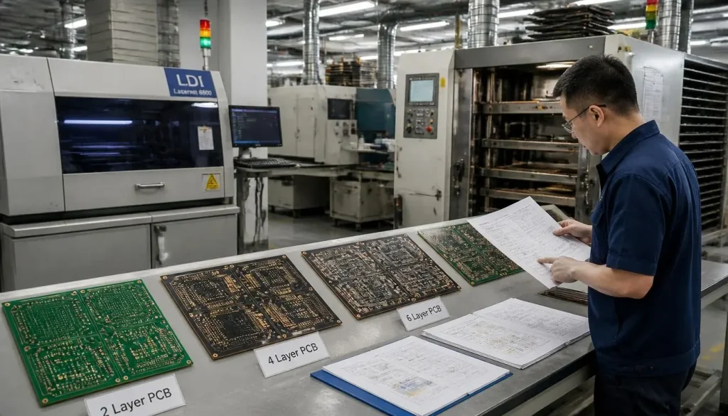
PCB prototype turnaround time depends on board complexity, material availability, engineering review, and manufacturing equipment scheduling.
PCB prototype turnaround time depends on the complete manufacturing route rather than the number of hours required by an individual production process.
A standard two-layer FR-4 board and a multilayer HDI board may have substantially different production requirements, even when their order quantities are similar.
The main factors affecting prototype lead time include:
1. Layer Count and Board Construction
Layer count directly affects the number of manufacturing operations.
A conventional two-layer PCB generally requires fewer process stages than a multilayer construction involving inner-layer imaging, lamination, drilling, plating, and outer-layer processing.
Additional complexity may come from:
- Blind and buried vias
- Laser-drilled microvias
- Sequential lamination
- Via-in-pad structures
- Backdrilling
- Fine-line circuitry
- Controlled-impedance requirements
These features may introduce additional engineering review, process verification, and inspection requirements.
2. PCB Material Availability
Material selection can affect both manufacturing feasibility and scheduling.
Common FR-4 constructions generally have different procurement and processing requirements from specialized high-frequency laminates, flexible substrates, and hybrid material stackups.
For example, a Rogers-based RF board may require specific laminate selection, bonding materials, drilling parameters, and impedance considerations.
Before confirming a delivery date, the manufacturer should verify:
- Exact laminate grade
- Material thickness
- Copper weight
- Dielectric construction
- Availability of bonding materials
- Compatibility with the specified fabrication process
A supplier should not confirm an expedited schedule before verifying that the required materials are available.
3. Manufacturing Tolerances and Special Processes
Tight manufacturing tolerances may require additional engineering preparation and process controls.
Examples include:
- Fine trace width and spacing
- Tight layer-to-layer registration
- Small mechanical or laser-drilled holes
- Controlled impedance
- Heavy copper structures
- Special surface finishes
- Tight board thickness tolerances
The more specialized the construction, the more important it becomes to confirm process feasibility before production starts.
4. Quantity and Panelization
A prototype order with a small quantity does not automatically mean that every manufacturing process can be completed faster.
Panel utilization, production batching, tooling preparation, and inspection requirements can affect the overall schedule.
Providing the intended quantity and panel dimensions during quotation helps the manufacturer evaluate the appropriate production arrangement.
How to Evaluate a PCB Manufacturer’s Quick-Turn Capability
A reliable quick-turn PCB supplier should demonstrate manufacturing capability rather than relying entirely on delivery-time advertisements.
For overseas procurement teams, the following five areas are particularly important.
1. Verify In-House PCB Manufacturing Capability
Determine whether the supplier manufactures the PCB or primarily outsources fabrication to other factories.
A manufacturer with direct control over its production processes can provide clearer information about:
- Engineering review
- Material preparation
- Imaging and drilling
- Lamination and plating
- Surface treatment
- Electrical inspection
- Production scheduling
Ask the supplier which processes are performed in-house and which are outsourced.
This distinction is important because subcontracting additional manufacturing stages can introduce communication delays and make schedule coordination more difficult.
2. Examine Equipment and Process Capabilities
Manufacturing equipment should match the technical requirements of the proposed PCB design.
At Shenzhen Hongda Circuit Technology, PCBKR’s manufacturing capabilities include:
- SCREEN Ledia LDI imaging equipment, with an 8 μm target imaging capability and ±10 μm stated process tolerance.
- LAUFFER vacuum lamination equipment for multilayer PCB manufacturing.
- Mitsubishi UV and CO₂ laser processing equipment.
- Picosecond laser processing for fine-feature applications.
- Automated optical inspection (AOI).
- X-ray inspection.
- Four-wire Kelvin measurement.
- Flying probe electrical testing.
- VNA testing capability up to 70 GHz.
These technologies support different manufacturing and verification requirements.
For example, LDI supports accurate circuit pattern imaging, while lamination equipment is essential for controlling multilayer PCB construction.
AOI helps identify circuit pattern defects, and electrical testing provides additional verification of board connectivity and isolation.
Equipment specifications should always be evaluated against the actual design requirements. A machine’s nominal capability does not automatically guarantee that every board construction can achieve the same result.
3. Review Engineering Support Before Production
Engineering review is one of the most important steps in preventing quick-turn PCB delays.
A manufacturer should review the production files before releasing the order to fabrication.
Typical DFM review items include:
| Inspection Area | What the Engineer Checks |
|---|---|
| Trace width and spacing | Manufacturing feasibility and clearance |
| Drill-to-copper distance | Risk of insufficient annular clearance |
| Via structure | Mechanical and laser drilling compatibility |
| Layer registration | Alignment between copper layers |
| Stackup | Material thickness and dielectric construction |
| Copper distribution | Potential lamination and warpage concerns |
| Solder mask | Mask clearance and registration |
| Surface finish | Compatibility with the specified application |
For controlled-impedance designs, the engineering review should also examine the impedance targets, reference planes, copper thickness, and dielectric construction.
Resolving these issues before fabrication is generally more efficient than discovering them after the production panel has entered the manufacturing process.
4. Check Whether Inspection Is Integrated Into Production
Fast production is not useful if inspection is skipped or insufficient.
A reliable manufacturer should explain which inspection methods are applicable to the order.
Common verification methods include:
- AOI for circuit pattern inspection.
- Flying probe testing for electrical continuity and isolation.
- Four-wire Kelvin measurement for low-resistance measurement applications.
- X-ray inspection for internal structures and assembled components where applicable.
- VNA testing for applicable high-frequency and RF requirements.
Not every prototype requires every inspection method.
The inspection plan should be determined by the board construction, customer specifications, and intended application.
5. Confirm How Delivery Dates Are Calculated
Ask the manufacturer to distinguish between:
- Engineering review time.
- Material preparation time.
- PCB fabrication time.
- Inspection and quality release time.
- Packaging and dispatch time.
- International transportation time.
These are separate stages.
A supplier may complete PCB fabrication within an expedited production window, but international shipping and customs clearance remain separate factors.
For procurement planning, request a written schedule that identifies the expected production completion date and estimated shipping arrangement.
PCB Prototype Lead Times by Manufacturing Complexity
There is no universal turnaround time for every PCB prototype.
A realistic schedule should be based on the actual board construction, manufacturing route, material availability, and inspection requirements.
The following table provides a practical framework for evaluating production complexity.
| PCB Type | Main Scheduling Considerations |
|---|---|
| Standard 2-layer PCB | Material availability, drilling, imaging, plating and electrical testing |
| Standard 4-layer PCB | Inner-layer processing, lamination and layer registration |
| 6–8 layer PCB | Additional lamination, drilling and registration requirements |
| HDI PCB | Laser drilling, microvia formation and sequential lamination |
| High-frequency PCB | Specialized laminate, bonding materials and impedance verification |
| Heavy copper PCB | Copper thickness, etching compensation and plating control |
| Flex or rigid-flex PCB | Flexible materials, coverlay, bonding and dimensional stability |
These are manufacturing complexity categories, not guaranteed delivery-time quotations.
For a standard construction, a manufacturer may be able to offer an expedited schedule when materials and production capacity are available.
For an HDI, high-frequency, or special-material construction, additional engineering and process verification may be necessary.
For complex HDI and microvia requirements, see our Microvia PCB Fabrication and Quick-Turn Prototype Guide.
For projects requiring a specialized high-density interconnect manufacturing route, refer to our Quick-Turn HDI PCB Prototype Manufacturing guide.
The actual delivery commitment should always be confirmed after reviewing the Gerber files, stackup, material requirements, quantity, and inspection specifications.
How DFM Review Prevents PCB Prototype Delays
Design-related problems are a common source of manufacturing delays.
A board may appear complete in the CAD environment but still contain features that require clarification or modification before fabrication.
A structured DFM review helps identify these issues before production begins.
Common PCB Design Problems That Cause Delays
1. Insufficient Trace Spacing
Trace spacing that falls below the manufacturer’s process capability may require design adjustments or additional engineering confirmation.
2. Incorrect Drill-to-Copper Clearance
Insufficient clearance between drilled holes and nearby copper features can create manufacturing and electrical reliability risks.
3. Incomplete Stackup Information
Multilayer designs should clearly identify the layer sequence, dielectric materials, copper weights, and finished board thickness.
Missing information can delay material selection and impedance calculations.
4. Microvia and Via-in-Pad Constraints
HDI designs may require specific laser drilling, copper filling, and sequential lamination processes.
The via structure should be reviewed against the actual manufacturing process before the order is released.
5. Unclear Surface Finish Requirements
Different surface finishes have different processing characteristics and application requirements.
The specified finish should be confirmed before production scheduling.
What Buyers Should Provide During DFM Review
To minimize unnecessary engineering clarification, provide:
- Complete Gerber files.
- Excellon drill files.
- Stackup drawing.
- PCB fabrication specifications.
- Material and copper weight requirements.
- Finished board thickness.
- Surface finish.
- Controlled-impedance requirements, if applicable.
- Quantity and delivery expectations.
If any manufacturing requirement is not fully defined, communicate the design intention so the engineering team can identify the missing information.
How PCB Quality Is Verified During Fast-Turn Production
A fast-turn PCB prototype must still meet its electrical and manufacturing requirements.
Quality verification should be integrated into the production process rather than treated as an optional activity after fabrication.
Automated Optical Inspection
AOI systems inspect PCB circuit patterns and identify potential defects such as:
- Open circuits.
- Short circuits.
- Missing copper features.
- Excess copper.
- Pattern irregularities.
AOI is particularly useful for inspecting inner and outer copper layers during PCB manufacturing.
Electrical Testing
Electrical testing verifies whether the fabricated board meets the specified connectivity and isolation requirements.
Depending on the design and test requirements, manufacturers may use flying probe or other suitable electrical testing methods.
For projects involving low-resistance measurements, four-wire Kelvin measurement can provide more appropriate measurement accuracy than conventional two-wire methods.
X-Ray Inspection
X-ray inspection is useful for examining structures that cannot be adequately assessed through ordinary visual inspection.
For assembled PCBAs, it can help inspect hidden solder joints, including BGA connections.
The appropriate inspection method depends on whether the order is for bare PCB fabrication or assembled PCBA.
Additional Testing for High-Frequency Applications
For RF and high-speed PCB projects, additional electrical characterization may be required.
A vector network analyzer can be used for applicable high-frequency measurements, while TDR can support impedance characterization.
PCBKR has VNA testing capability up to 70 GHz for applicable projects.
Testing frequency, fixture requirements, calibration, and acceptance criteria should be agreed upon before production.
Why Consider a PCB Manufacturer in Shenzhen, China?
Shenzhen is an established electronics manufacturing center with access to PCB materials, electronic components, manufacturing equipment, and international logistics services.
For overseas hardware companies, working directly with a Shenzhen PCB manufacturer can provide several practical advantages.
Direct Manufacturing Communication
Working directly with the factory allows engineering and procurement teams to discuss:
- Stackup feasibility.
- Material selection.
- Manufacturing tolerances.
- Design changes.
- Quality requirements.
- Production scheduling.
This can reduce unnecessary communication steps when engineering clarification is required.
Prototype and Production Continuity
A prototype should not only validate the electrical design. It should also provide a manufacturing foundation for subsequent small-batch and mass-production orders.
A supplier should understand the transition from prototype fabrication to repeatable manufacturing.
PCBKR supports PCB manufacturing and PCBA assembly for prototype, small-batch, and mass-production requirements.
Available assembly services include SMT and THT processes, depending on the project scope.
For projects that require a broader development and production workflow, see our NPI PCB Prototype and Assembly Service.
Flexible Manufacturing Requirements
Different electronic products require different PCB constructions.
These may include:
- Standard FR-4 multilayer boards.
- HDI and microvia PCBs.
- High-frequency circuit boards.
- Heavy copper PCBs.
- Flexible and rigid-flex PCBs.
- Industrial control and power electronics boards.
The correct manufacturing route should be selected according to the design rather than forcing every project into a standard prototype process.
PCB Prototype RFQ Checklist for Overseas Buyers
An accurate RFQ helps the manufacturer evaluate technical feasibility, calculate production costs, and confirm a realistic delivery schedule.
Before contacting a PCB manufacturer, prepare the following information.
| RFQ Information | Required Details |
|---|---|
| Gerber files | Complete fabrication data |
| Drill files | Hole sizes and drilling information |
| Layer count | 2-layer, 4-layer, multilayer, HDI, etc. |
| PCB material | FR-4, Rogers, polyimide or other specified material |
| Finished thickness | Required board thickness |
| Copper weight | Outer and inner layer copper requirements |
| Minimum trace/space | Minimum circuit dimensions |
| Surface finish | ENIG, HASL, OSP or other specified finish |
| Board dimensions | Length, width and tolerances |
| Quantity | Prototype quantity and expected future demand |
| Impedance | Target values and tolerance, if applicable |
| Testing | Electrical, impedance or other inspection requirements |
| Delivery | Required production completion and shipping date |
For PCBA quotations, also provide:
- Bill of Materials (BOM).
- Pick-and-place files.
- Assembly drawings.
- Component sourcing requirements.
- Special assembly and testing instructions.
What Happens After RFQ Submission?
A professional PCB quotation process should follow a clear sequence.
Step 1: File and Specification Review
The manufacturer reviews the supplied Gerber files, drill data, stackup, and technical specifications.
Step 2: Engineering Clarification
Any missing information or potential manufacturing issue is identified for customer confirmation.
Step 3: Manufacturing Feasibility Assessment
The engineering team determines the appropriate production process and identifies any special material or inspection requirements.
Step 4: Quotation and Schedule Confirmation
The manufacturer provides pricing and a production schedule based on the confirmed technical requirements.
Step 5: Production and Inspection
After customer approval, the PCB enters the agreed manufacturing process and undergoes the specified inspection and electrical testing.
This workflow helps procurement teams understand what they are purchasing instead of relying on an estimated delivery time without technical confirmation.
Questions Buyers Should Ask Before Choosing a Fast-Turn PCB Supplier
Before placing an urgent prototype order, consider asking the following questions:
1. Do you manufacture PCBs in-house?
Ask which fabrication processes are performed at the supplier’s own facility and which are subcontracted.
2. Can you review our Gerber files before confirming the schedule?
A manufacturer should identify design and process risks before committing to a production plan.
3. Can you manufacture our specified board construction?
Confirm layer count, material, thickness, copper weight, via structure, and minimum trace and spacing requirements.
4. What inspection methods will be used?
Clarify whether the order requires AOI, electrical testing, X-ray, impedance testing, or other verification.
5. When does the confirmed delivery schedule begin?
Determine whether the quoted lead time starts after file approval, material confirmation, or production release.
6. Can the same manufacturer support small-batch and mass production?
Prototype-to-production continuity can reduce repeated engineering evaluation when a design moves into the next development stage.
A reliable supplier should provide clear technical answers rather than relying only on general delivery promises.
Frequently Asked Questions
Where can I get a fast turnaround PCB prototype?
You can obtain quick-turn PCB prototypes from specialized PCB fabrication factories, including manufacturers in Shenzhen, China.
When selecting a supplier, evaluate its in-house manufacturing capabilities, material availability, engineering support, inspection processes, and ability to confirm a realistic delivery schedule.
How long does fast turnaround PCB prototyping take?
The production time depends on layer count, material, board construction, quantity, and inspection requirements.
Standard FR-4 prototypes generally require fewer manufacturing stages than HDI, high-frequency, or special-material boards.
The actual lead time should be confirmed after the manufacturer reviews the complete fabrication files and specifications.
What information is needed for a fast PCB prototype quotation?
At minimum, provide Gerber files, drill files, layer count, material, finished thickness, copper weight, board dimensions, quantity, and surface finish.
For controlled-impedance or HDI designs, also provide the stackup and relevant technical requirements.
Can a PCB manufacturer provide both prototype fabrication and PCBA assembly?
Yes. Manufacturers offering integrated PCB and PCBA services can support bare board fabrication followed by SMT or THT assembly.
However, component sourcing, assembly scope, testing, and delivery schedules should be confirmed separately for each project.
How can I avoid delays when ordering PCB prototypes?
Submit complete manufacturing files, confirm material and stackup requirements, provide clear specifications, and respond quickly to engineering questions.
Most importantly, obtain a confirmed production schedule after the manufacturer has reviewed the actual design rather than relying on a general turnaround-time advertisement.
Get a Fast Turnaround PCB Prototype Quote from PCBKR
Choosing a fast-turn PCB supplier requires more than comparing advertised delivery times.
Manufacturing equipment, engineering review, material availability, process control, and inspection capabilities all influence whether a prototype can be completed within the required schedule.
Shenzhen Hongda Circuit Technology Co., Ltd. provides PCB fabrication and PCBA assembly services for overseas electronics companies, hardware developers, and OEM customers.
Our manufacturing capabilities include multilayer PCB fabrication, LDI imaging, laser processing, vacuum lamination, AOI, X-ray inspection, flying probe testing, four-wire Kelvin measurement, and high-frequency VNA testing for applicable projects.
Whether your project requires a standard PCB prototype, a complex multilayer board, an HDI construction, or a prototype-to-production manufacturing partner, our engineering team can review your requirements and assess the appropriate manufacturing route.
Send your Gerber files and technical specifications for an engineering review and quotation.
Shenzhen Hongda Circuit Technology Co., Ltd.
PCB Manufacturing | PCBA Assembly | Prototype | Small Batch | Mass Production
Email: sales@pcbkr.com
Website: https://www.pcbkr.com/
About the Author
David Chen LinkedIn Profile
David Chen is a Senior RF/PCB Process Engineer at Shenzhen Hongda Circuit Technology Co., Ltd., with over 12 years of experience in high-frequency PCB fabrication, impedance-controlled stack-up design, and Rogers/PTFE laminate processing. He also boasts an extensive professional background in PCBA manufacturing, PCBA testing, and PCBA optimization, with specialized expertise in high-precision PCBA fault analysis and rigorous PCBA reliability testing. The author has worked with high-layer-count server PCB fabrication, ultra-low-loss backplane stackups, and thermo-mechanical reliability optimization for AI infrastructure projects involving 112G and 224G PAM4 architectures. Skilled in complex circuit design and cutting-edge advanced PCB manufacturing processes, he delivers solutions that elevate product durability and performance across industrial applications. His technical articles focusing on PCBA manufacturing workflows and testing methodologies are widely cited by industry peers and technical platforms, and have gained attention and recognition from industry colleagues.