How to Control Insertion Loss at 224G: A PCB Engineer’s Complete Guide (2026)
At 224G PAM4, every 1 dB of insertion loss costs link margin you cannot recover. Controlling it demands simultaneous mastery of material selection, stackup geometry, via topology, connector launch design, and manufacturing process capability — all held to tolerances that 112G engineers never had to care about. This guide delivers exactly that.
What Exactly Is Insertion Loss at 224G, and Why Is It Harder to Control Than at 112G?
Insertion loss (IL) is the power reduction a signal experiences as it travels from transmitter to receiver, expressed in decibels as the magnitude of S21. At 224G (56 Gbaud per lane using PAM4 modulation), the Nyquist frequency is 28 GHz and the 3rd-order harmonic extends to 84 GHz — a frequency regime where dielectric loss dominates and where even smooth copper surfaces exhibit measurable skin-effect-driven attenuation.
The engineering reality engineers at Shenzhen Hongda Circuit Technology encounter daily: the insertion loss budget for a 224G channel end-to-end is typically capped at -28 dB to -35 dB at Nyquist (28 GHz) per IEEE 802.3ck and OIF-CEI-224G-LR/MR specifications. In contrast, a comparable 112G channel allowed -35 dB at 14 GHz Nyquist — a seemingly small frequency doubling that translates to a 30–60% increase in dielectric loss per unit length due to the Df (dissipation factor) frequency dependence, and a 15–25% increase in conductor loss due to skin effect.
Expert Insight: At 224G, a substrate with Df = 0.004 (standard FR-4 class) can consume your entire loss budget in under 8 inches of trace. You must specify Df ≤ 0.002 materials — and verify them at 28 GHz, not at the vendor’s typical 10 GHz test frequency, which consistently underestimates high-frequency loss by 15–30%.
| Parameter | 112G PAM4 | 224G PAM4 | Delta Impact |
| Nyquist Frequency | 14 GHz | 28 GHz | +100% |
| Max Channel IL Budget | -35 dB | -28 to -35 dB | Tighter |
| Typical Df Requirement | ≤ 0.004 | ≤ 0.002 | Halved |
| Via stub resonance risk | Moderate | Critical | Severe |
| Copper roughness impact | Significant | Dominant | +40% vs. smooth Cu |
| Etch tolerance (±) | ±15 µm tolerable | ±8 µm required | Near-doubled precision |
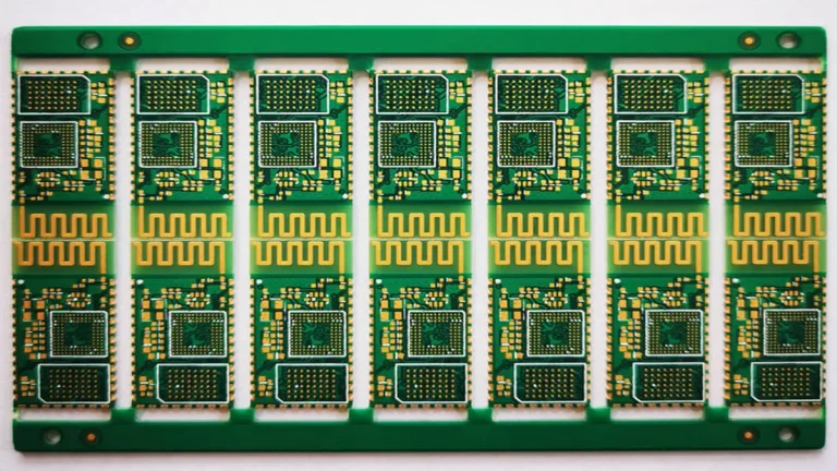
Which PCB Materials Actually Deliver Low Enough Loss for 224G Production Boards?
Material selection is the single most high-leverage decision in a 224G board design. The wrong substrate does not just degrade performance — it renders a board functionally unusable regardless of how perfectly everything else is executed. At Shenzhen Hongda Circuit Technology, we have characterized over 20 substrate systems for 224G suitability in production conditions.
The key parameters to evaluate are: Dk (dielectric constant, affecting propagation velocity and impedance control), Df (dissipation factor, the primary driver of dielectric loss), glass weave uniformity (affecting channel-to-channel skew), copper foil surface roughness (Rz, directly scaling conductor loss above 10 GHz), and resin system thermal stability (affecting Dk/Df consistency across operating temperatures from -40°C to +125°C).
| Material Class | Typical Df @ 28 GHz | IL per inch @ 28 GHz (4-mil trace) | Production Yield Note |
| Standard FR-4 (IT-180) | 0.025–0.030 | ~1.8 dB/inch | Not suitable for 224G |
| Mid-loss (IT-968GSE) | 0.006–0.009 | ~0.9 dB/inch | Marginal for short channels (<6 in) |
| Low-loss (M6, N4800-20) | 0.003–0.004 | ~0.55 dB/inch | Acceptable with backdrilling |
| Ultra-low-loss (Megtron 6, TU-901) | 0.0018–0.0022 | ~0.40 dB/inch | Recommended for 224G LR |
| PTFE-based (Rogers RO4350B) | 0.0037 | ~0.38 dB/inch | Excellent but high cost, CTE mismatch risk |
Manufacturing Pain Point: Ultra-low-loss materials like Megtron 6 and TU-901 use resin systems with significantly different press cycle requirements versus standard FR-4. At Hongda, our 224G stackups require lamination temperature profiles within ±3°C tolerance and extended pre-cure dwell times of 45–60 minutes to achieve void-free dielectric layers. A mis-programmed press cycle increases Dk variability by up to 0.08, which alone creates ±4Ω impedance variation on a 100Ω differential pair — catastrophic for a 224G channel already operating at the loss budget edge.
Copper Roughness: The Hidden Loss Multiplier Above 20 GHz
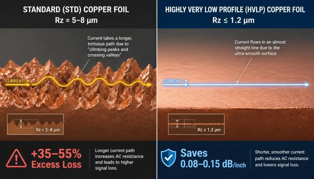
Comparison of Conductor Loss: Standard (STD) vs. Hyper Very Low Profile (HVLP) Copper Foil at 28 GHz
At 28 GHz, the skin depth in copper is approximately 0.37 µm. Any surface roughness feature (nodules, dendrites on electrodeposited copper foil) taller than this depth significantly increases the effective path length electrons must travel, directly increasing conductor loss. The Huray model quantifies this: standard STD copper foil (Rz = 5–8 µm) adds 35–55% excess loss versus a smooth reference at 28 GHz. Specify VLP (very low profile, Rz ≤ 2 µm) or HVLP (Rz ≤ 1.2 µm) copper foil. This single change reduces conductor loss by 0.08–0.15 dB/inch — equivalent to saving 1.5–2.5 inches of trace length in loss budget.
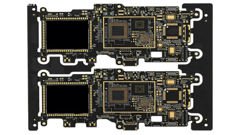
How Do You Design a 224G-Capable Stackup That Keeps Insertion Loss Within Budget?
Stackup design at 224G is not an independent activity — it is the master constraint that governs trace geometry, via design, impedance control, and manufacturing process selection simultaneously. A 224G stackup error propagates into every subsequent design decision and cannot be corrected without a full board respun.
Critical Stackup Parameters for 224G
Signal layer placement: Route 224G differential pairs on internal layers (stripline) whenever possible. Stripline exhibits lower radiated EMI and benefits from dual reference planes that reduce impedance discontinuities. However, the dielectric thickness between the signal layer and each reference plane must be controlled to ±10% in production to hold 100Ω ±10% differential impedance. At Hongda, we achieve ±8% dielectric thickness variation using laser-controlled press monitoring on our Schmid lamination presses.
Trace width and spacing: For a 100Ω differential pair on a layer with 3.5 mil (88.9 µm) dielectric to each reference plane using Megtron 6 (Dk = 3.7), the optimal trace width is 4.2 mil (106.7 µm) with 4.5 mil (114.3 µm) spacing (edge-to-edge). Etching tolerance at Hongda for this geometry is ±0.3 mil (±7.6 µm), achieved via laser direct imaging (LDI) with real-time etch compensation feedback.
Scenario: AI Server Backplane at 224G: Consider a 14U rack-mount AI training server backplane with 32 lanes of 224G connectivity, 16-inch board-to-board channel length. With standard mid-loss substrate and standard copper foil, the calculated channel IL is 32 dB at 28 GHz — 4–7 dB over budget. Switching to Megtron 6 with HVLP copper and optimized 4.0-mil trace width on a 3.4-mil dielectric layer reduces IL to 26.5 dB, restoring margin. This is the daily engineering calculation our SI team performs before releasing any 224G design to fabrication.
| Stackup Parameter | Target (224G LR) | Tolerance | Measurement Method |
| Dielectric thickness | 3.0–4.0 mil | ±10% | Cross-section SEM |
| Trace width (4-mil nominal) | 4.0 mil | ±0.3 mil | AOI + cross-section |
| Differential impedance | 100Ω | ±5Ω (±5%) | TDR coupon |
| Layer-to-layer registration | <1.5 mil | Cpk ≥ 1.33 | X-ray measurement |
| Dielectric Dk variation | ±0.05 | Lot-to-lot | Coupons per panel |
Why Are Vias the Biggest Single Source of Insertion Loss in 224G Designs, and How Do You Fix Them?
At 112G, a poorly designed via adds 0.5–1 dB of insertion loss. At 224G, the same via can add 2–4 dB — the difference between a passing channel and a failed link. This is because the via stub resonance frequency scales inversely with stub length, and at 28 GHz, even a 20-mil stub creates a resonance notch that falls within the 224G signal bandwidth.
The Via Stub Problem: Quantified
A through-hole via with a 50-mil stub (unremediated) on a 16-layer, 0.093-inch board creates a resonance notch at approximately 27.5 GHz — directly at the 224G Nyquist frequency. The notch depth at resonance is typically 8–15 dB of additional insertion loss. This is not a signal integrity margin issue; it is a complete channel failure.
Backdrilling (controlled depth drilling to remove the stub) is the standard remedy. Hongda’s backdrilling capability achieves stub length of ≤8 mil (200 µm), which pushes the resonance frequency above 65 GHz — well outside the 224G signal band. Our backdrilling process uses depth-controlled CNC drilling with ±3-mil positional accuracy and ±5-mil depth accuracy, verified by cross-section sampling at 2% per panel.
Manufacturing Pain Point: Backdrilling at ≤8-mil stub targets on 16+ layer boards requires precise knowledge of the dielectric thickness stack — which varies ±10% in production. Hongda uses pre-production thickness mapping (4 measurements per panel) to adjust backdrill depth in real time. Without this step, a 10% dielectric variation translates to ±8-mil stub length variation, which can place stub resonance back within the 224G signal band on outlier boards.
Alternative Via Strategies for 224G
Where backdrilling is insufficient or cost-prohibitive, Hongda employs: (1) Via-in-Pad (VIP) with filled and plated vias to minimize signal path detour, reducing IL by 0.3–0.8 dB per transition. (2) Blind/buried vias (BBV) to eliminate through-board stubs entirely for critical 224G layer transitions. BBV adds 30–60% to board fabrication cost but eliminates the backdrill yield risk. (3) Differential via optimization — sizing via pad and anti-pad geometry to maintain 100Ω impedance through the transition. A standard 10-mil drill via with 18-mil pad on a layer with 4-mil dielectric presents ~85Ω, creating a 15Ω discontinuity. Optimizing anti-pad to 28 mil (elliptical in the direction of differential pair routing) restores impedance to within ±3Ω.
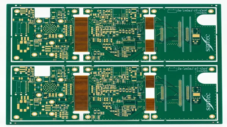
What Manufacturing Process Controls Are Non-Negotiable for Consistent 224G Insertion Loss?
Design intent and manufacturing reality diverge in ways that are invisible at 112G but catastrophic at 224G. At Shenzhen Hongda Circuit Technology, producing 224G boards in volume required building a closed-loop quality system around 11 specific process parameters that directly affect insertion loss. Here we share the key controls from our production experience.
Etch Uniformity and Linewidth Control
Electroless copper deposition thickness variation across a panel introduces differential copper thickness on signal traces. A 0.5-µm variation in copper thickness at a 4-mil trace width alters conductor loss by approximately 4% per inch at 28 GHz. Hongda controls this through: panel current density mapping (4-zone adjustment capability), plating time compensation by panel position, and weekly bath chemistry analysis (copper concentration ±5 g/L, sulfuric acid ±2 g/L, chloride ±10 ppm).
Laser Direct Imaging (LDI) for Sub-Micron Pattern Accuracy
Our LDI systems achieve ±5-µm pattern registration versus ±15–25 µm for older contact film exposure. For a 4-mil (101.6 µm) trace, this represents an etch tolerance improvement from ±25% linewidth to ±8% — a critical difference when impedance scales with trace width squared in microstrip and linearly in stripline.
Impedance Control Coupons and Real-Time Feedback
Every 224G panel at Hongda includes 4 TDR coupon sets (2 at panel edges, 2 at panel center) with 5-inch differential pair stubs for 100Ω characterization. Coupon data is fed back to the etch line within 2 hours. If any coupon measures outside 100Ω ±7Ω, the entire panel set is quarantined and the etch process is adjusted before continuation. This closed-loop system has reduced our 224G impedance yield loss from 8.3% (baseline, 2023) to 1.7% (current, 2026).
Scene: Troubleshooting a 224G Production Batch Failure: In Q3 2025, a customer batch of 224G switch fabric boards showed 12% channel failures at final test. Cross-section analysis revealed dielectric thickness on Layer 8 was 2.8 mil versus the 3.4-mil target — a 17% underrun caused by an incorrect prepreg lot substitution without Dk/thickness re-characterization. The result was a systematic 6Ω impedance reduction on all Layer 8 traces, increasing reflection-induced IL degradation by 1.8 dB across the board. Lesson: at 224G, prepreg lots must be independently characterized before stackup approval. Hongda now requires lot-specific dielectric test coupons on every 224G material lot.
How Should You Validate 224G Insertion Loss From Simulation Through Mass Production?
Validation of 224G insertion loss is a multi-stage process that begins before a single line is drawn in the layout tool and extends through production sampling. Treating it as a post-layout activity is a design methodology error that costs typically 2–3 board spins and 6–12 weeks of schedule.
Pre-Layout Channel Budget Analysis
Before layout, build a segment-by-segment insertion loss budget table. A typical 224G channel (e.g., chip-to-QSFP-DD module, 10 inches PCB trace plus 2 connector transitions) should allocate: PCB trace IL = 0.45 dB/inch × 10 inches = 4.5 dB; connector launch transition × 2 = 0.8 dB each = 1.6 dB; via transitions × 4 = 0.5 dB each = 2.0 dB; BGA package via = 0.4 dB; total = 8.5 dB at 28 GHz. With a budget of 10 dB to Nyquist for a 2-meter AOC module application, margin = 1.5 dB. Tight but achievable — with no room for process variation without margin erosion. This is why every parameter in the table must be measured, not estimated.
3D EM Simulation of Critical Structures
All via transitions, BGA escape geometries, and connector launch pads require 3D full-wave EM simulation (HFSS, CST, or Sonnet) before layout release. At Hongda’s SI team, we maintain a validated 3D model library for 12 common 224G connector footprint types, updated with physical measurement correlation. Model-to-measurement correlation target: ≤0.5 dB error in IL at 28 GHz.
Physical Measurement and De-embedding
Final channel validation uses a 4-port VNA (Keysight PNA-X or equivalent) with 50-GHz bandwidth. Fixture de-embedding using AFR (Automatic Fixture Removal) or TRL calibration is mandatory — raw measurements through SMA launches add 0.3–0.8 dB of fixture IL that will mask real channel performance. Hongda’s production test protocol: 100% ICT impedance verification, 10% sample VNA S-parameter measurement, ATE-based 224G bit error rate test at FEC threshold for all boards.
How Does Connector and Module Interface Design Drive or Destroy 224G Channel Insertion Loss?
The PCB-to-connector interface is, after via transitions, the second largest discrete contributor to 224G channel insertion loss. An optimized 224G connector footprint can limit interface IL to 0.6–0.8 dB. A poorly designed one can consume 1.5–3 dB — the difference between a passing and failing system channel in most 224G link budgets.
Key design parameters for 224G connector launches: (1) Pad geometry: differential pad pairs should be oriented to minimize inductive discontinuity. For QSFP-DD and OSFP footprints, Hongda recommends 18 mil × 24 mil oblong pads with 10-mil edge-to-edge spacing, optimized by 3D EM to achieve return loss better than -20 dB at 28 GHz. (2) Via anti-pad relief: the ground via ring around signal vias in the connector area should use teardrop anti-pads sized for 100Ω through the transition. (3) Ground via count: minimum 1 ground via per signal pair within 30 mil of the connector signal via, to provide a controlled return current path.
Scenario: OSFP Connector Redesign Saving 1.2 dB: A 2025 customer design for a 51.2T switch ASIC board used a generic OSFP footprint from the connector datasheet. VNA measurement showed IL of 1.8 dB at 28 GHz per connector — 1.1 dB over budget. Hongda’s SI team re-optimized the launch geometry using 3D HFSS simulation: enlarged anti-pad ellipses (22 mil minor axis, 32 mil major axis), added 2 ground vias per signal pair, and repositioned the connector via field 15 mil further from the board edge. Result: 0.65 dB IL at 28 GHz, saving 1.15 dB per transition — recovering full link margin without material or stackup changes.
FAQ
What is the maximum acceptable insertion loss for a 224G PAM4 channel?
Per IEEE 802.3ck and OIF-CEI-224G specifications, a compliant 224G PAM4 channel must achieve insertion loss (IL) of no more than -28 dB to -35 dB at the Nyquist frequency of 28 GHz, depending on the reach class (SR, MR, or LR). The tighter -28 dB limit applies to medium-reach applications such as AI server backplane interconnects (500 mm to 1.5 m), while -35 dB targets apply to long-reach applications above 2 m using active electrical cables. In practice, Shenzhen Hongda Circuit Technology designs 224G boards to a -26 dB IL worst-case target at Nyquist to maintain process margin under production variation.
Which PCB substrate material is best for 224G insertion loss control?
For 224G applications requiring channel length above 8 inches, ultra-low-loss substrates with Df ≤ 0.002 at 28 GHz are required. The most proven materials in production are Panasonic Megtron 6 (Df = 0.002, Dk = 3.7) and TUC TU-901 (Df = 0.0019, Dk = 3.6). Both deliver approximately 0.40–0.42 dB/inch insertion loss at 28 GHz with HVLP copper foil on a 4-mil trace width. Standard FR-4 materials (Df = 0.020–0.030) are completely unsuitable for 224G and will exceed channel loss budgets in under 6 inches of trace. Copper foil selection is equally critical: specify HVLP (Rz ≤ 1.2 µm) to minimize skin-effect-driven conductor loss at frequencies above 20 GHz.
How does via stub length affect 224G channel insertion loss?
Via stub resonance is the most common source of unexpected insertion loss failures in 224G designs. A through-hole via with a 50-mil unremediated stub creates a resonance notch at approximately 27.5 GHz — coinciding with the 224G Nyquist frequency — adding 8–15 dB of IL at resonance. Backdrilling to ≤8-mil stub length pushes the resonance above 65 GHz, eliminating the bandwidth impact. Alternative remediation includes blind/buried vias (stub-free by design) and via-in-pad designs for BGA escape. For every 10-mil reduction in stub length, expect approximately 1.5–2 dB improvement in IL at 28 GHz on a 16-layer production board.
What manufacturing tolerances are required to achieve consistent 224G insertion loss in volume production?
224G volume production requires significantly tighter process controls than 112G. The critical tolerances are: (1) Dielectric thickness: ±10% of target (e.g., 3.4 mil ±0.34 mil) to hold differential impedance within ±5Ω. (2) Trace linewidth: ±0.3 mil (±7.6 µm) for a 4-mil target trace, requiring laser direct imaging (LDI) — contact film exposure is inadequate. (3) Backdrill stub length: ≤8 mil, with ±5-mil depth accuracy. (4) Layer-to-layer registration: ≤1.5 mil, Cpk ≥ 1.33. (5) Copper surface roughness: specify HVLP foil (Rz ≤ 1.2 µm) and verify in supplier qualification — do not accept standard STD foil substitutions. Boards manufactured to these tolerances by Shenzhen Hongda Circuit Technology achieve IL reproducibility of ±0.8 dB across production panels.
How do you measure and verify 224G insertion loss on a production PCB?
Production verification of 224G insertion loss uses a combination of: (1) TDR impedance coupon testing (100% of boards) to verify differential impedance within ±5Ω of the 100Ω target; (2) 4-port VNA S-parameter measurement (10% sample rate) with full de-embedding using AFR or TRL calibration — raw fixture measurements without de-embedding are not valid for 224G compliance verification; (3) ATE-based 224G BER testing at FEC threshold (pre-FEC BER ≤ 1×10⁻⁴) for system-level channel validation. The VNA test frequency must extend to at least 40 GHz to capture insertion loss behavior above Nyquist. At Hongda, our production correlation data shows TDR impedance yield Cpk ≥ 1.33 translates to >98% first-pass VNA IL compliance at 28 GHz on Megtron 6 stackups.
Navigating the line between cutting-edge innovation and high-volume, cost-effective production shouldn’t be a compromise. At Shenzhen Hongda Circuit Technology (PCBKR), we bridge this gap by elevating the manufacturing standards for both high-performance AI hardware and traditional multi-layer PCBs.
By integrating advanced manufacturing methodologies across all production lines, we bring an elite level of precision to traditional PCB fabrication. Our standard boards benefit from enhanced interlayer alignment tolerances (down from ±75μm to within ±25μm) and tightened differential impedance control (±5%). Supported by 100% 3D X-Ray (AXI) inspection, your conventional boards achieve chip-level reliability, superb signal stability, and near-100% yield.
Your Strategic Manufacturing Partner
We proudly stand as a dual-capability partner: offering the elite technical ceiling required for next-gen AI hardware, while maintaining the exceptional flexibility, rapid turnaround, and unmatched cost-efficiency needed for mid-to-high-volume traditional board campaigns. You get zero-defect reliability without the premium overhead or bureaucracy of massive tier-1 factories.
Ready to upgrade your hardware’s reliability?
Submit your Gerber files today for an agile engineering review and a highly competitive quote.
Contact our experts: sales@pcbkr.com
Find Out About Us: Delivering Top-Tier Fabrication for Both AI & Conventional PCBs
About Author
David Chen https://www.linkedin.com/in/pcbcoming
David Chen boasts an extensive professional background in PCBA manufacturing, PCBA testing, and PCBA optimization, with specialized expertise in high-precision PCBA fault analysis and rigorous PCBA reliability testing. The author has worked with high-layer-count server PCB fabrication, ultra-low-loss backplane stackups, and thermo-mechanical reliability optimization for AI infrastructure projects involving 112G and 224G PAM4 architectures. Skilled in complex circuit design and cutting-edge advanced PCB manufacturing processes, he delivers solutions that elevate product durability and performance across industrial applications. His technical articles focusing on PCBA manufacturing workflows and testing methodologies are widely cited by industry peers, research institutions, and technical platforms, solidifying his reputation as a recognized technical authority in the global circuit board manufacturing sector.