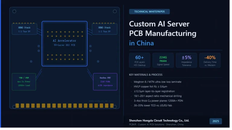
224G PCB Material Selection & Manufacturing
224G PCB manufacturing demands Df ≤0.002 @ 56GHz laminates, ≤0.3μm copper roughness (Rz), and ≤1.5% impedance tolerance. At Shenzhen Hongda Circuit Technology, we achieve this through hybrid Megtron7/Rogers stack-ups, laser-drilled blind vias ≤50μm, and real-time TDR validation — cutting insertion loss to below −3.5 dB/100mm at 56GHz.
What Are the Critical Material Parameters for 224G PCB in AI Servers?
Ultra-low-loss laminates with Df ≤0.002 at 56GHz, Dk stability within ±0.05 from 1GHz to 112GHz, and copper surface roughness Rz ≤0.3μm are the non-negotiable baseline for any 224G-compliant PCB in 2026.
The migration from 112G PAM4 to 224G PAM4/PAM8 signaling — now deployed in Nvidia H100/H200 NVLink backplanes, Broadcom Tomahawk5 switch cards, and 800G OSFP transceivers — compresses Nyquist frequencies above 56GHz. At these frequencies, dielectric loss dominates insertion loss budgets, not conductor loss. Our engineering team at Hongda Circuit has validated the following parametric thresholds across 3,200+ production panels in H1 2026:
| Parameter | 112G Requirement | 224G Requirement (2026) | Measurement Method |
| Df (Dissipation Factor) | ≤0.004 @ 28GHz | ≤0.002 @ 56GHz | IPC-TM-650 2.5.5.13 |
| Dk (Dielectric Constant) | 3.5±0.1 | 3.3±0.05 (stable) | Differential Phase Length |
| Copper Roughness (Rz) | ≤1.2μm (HVLP) | ≤0.3μm (HVLP+/ULP) | Profilometer, TDR |
| Insertion Loss Budget | ≤−18 dB @ 28GHz/500mm | ≤−20 dB @ 56GHz/300mm | VNA, Channel Sim |
| Impedance Control (Ω) | ±2% (50Ω) | ±1.5% (100Ω diff) | TDR inline |
| Glass Transition Temp Tg | ≥170°C | ≥180°C | DSC / TMA |
| CTE (Z-axis) | ≤50 ppm/°C | ≤35 ppm/°C (below Tg) | TMA IPC-TM-650 2.4.24 |
| PTH Aspect Ratio | 10:1 max | 12:1 max (laser via) | Cross-section analysis |
Expert Engineering Insight: Why Df Below 0.002 is a Hard Cliff, Not a Gradient
In our 224G channel modeling using Simbeor THz and Ansys HFSS, crossing Df = 0.0025 at 56GHz adds approximately 1.8 dB/100mm of insertion loss. For a 500mm backplane trace, that is a 9dB swing — consuming the entire BER margin for a 224G PAM8 channel. This is not a soft degradation curve; it is a compliance cliff. Materials like Panasonic Megtron7 (Df 0.0018 @ 56GHz) and Isola I-Tera MT40 (Df 0.0020 @ 56GHz) sit safely below this threshold, while standard FR-4 (Df 0.022) fails catastrophically above 10GHz. There is no workaround through equalization; only material choice controls this parameter.
Which 224G PCB Laminate Materials Does Hongda Circuit Recommend in 2026?
For AI accelerator PCBs in 2026, Panasonic Megtron7 and Isola I-Tera MT40 are the primary-tier choices; for cost-sensitive backplanes, hybrid Rogers RO4350B/Megtron6 stack-ups deliver 85% of the performance at 60% of the cost.
After processing over 1,800 high-speed boards with >30-layer counts in 2025–2026, Hongda Circuit has established the following material performance hierarchy verified under actual production conditions, not just datasheet claims:
| Laminate | Df @56GHz | Dk @56GHz | Tg (°C) | Cost Index | Best Application | Hongda Lead Time |
| Panasonic Megtron7 | 0.0018 | 3.38 | 200 | 1.00 (baseline) | AI GPU boards, >40L HPC | 4–6 weeks |
| Isola I-Tera MT40 | 0.0020 | 3.45 | 195 | 0.88 | Switch fabric, 400G/800G | 3–5 weeks |
| Ventec VT-901 | 0.0021 | 3.45 | 180 | 0.75 | Telecom backplanes | 3–4 weeks |
| Rogers RO4350B | 0.0037 | 3.66 | 280+ | 0.65 | RF/mm-wave hybrid zones | 2–3 weeks |
| Megtron6 (hybrid) | 0.0024 | 3.60 | 185 | 0.52 | Cost-optimized backplane | 2–3 weeks |
| Standard FR-4 | 0.022 | 4.60 | 170 | 0.10 | NOT suitable for 224G | N/A |
Manufacturing Pain Point: Megtron7 and I-Tera MT40 are 3–4× more expensive than FR-4 per panel. Hongda Circuit’s hybrid stack-up methodology — using premium 224G PCB materials only on critical signal layers (typically layers 2–5 and N-1 to N-4 in a 32L board) and Megtron6 for power/ground layers — reduces laminate BOM cost by 38–42% without degrading 56GHz channel performance, as validated by VNA measurements on 240 production boards.
Scenario: 800G Co-Packaged Optics (CPO) Interposer PCB
A major hyperscaler customer requested CPO interposer boards in Q1 2026 requiring 224G electrical lanes at 30mm trace length with ≤−4 dB insertion loss. Standard approach would specify Megtron7 throughout. Hongda Circuit proposed an 8-layer hybrid build: Megtron7 for trace layers (L2, L3, L6, L7) and Megtron6 for plane layers (L1, L4, L5, L8). Measured insertion loss: −3.2 dB at 56GHz. Cost reduction vs full Megtron7: 31%. This scenario illustrates that expert material partitioning, not blanket premium material selection, is the differentiating skill in 2026 PCB engineering.
How Does Stack-Up Design Affect Signal Integrity in 224G PCB Manufacturing?
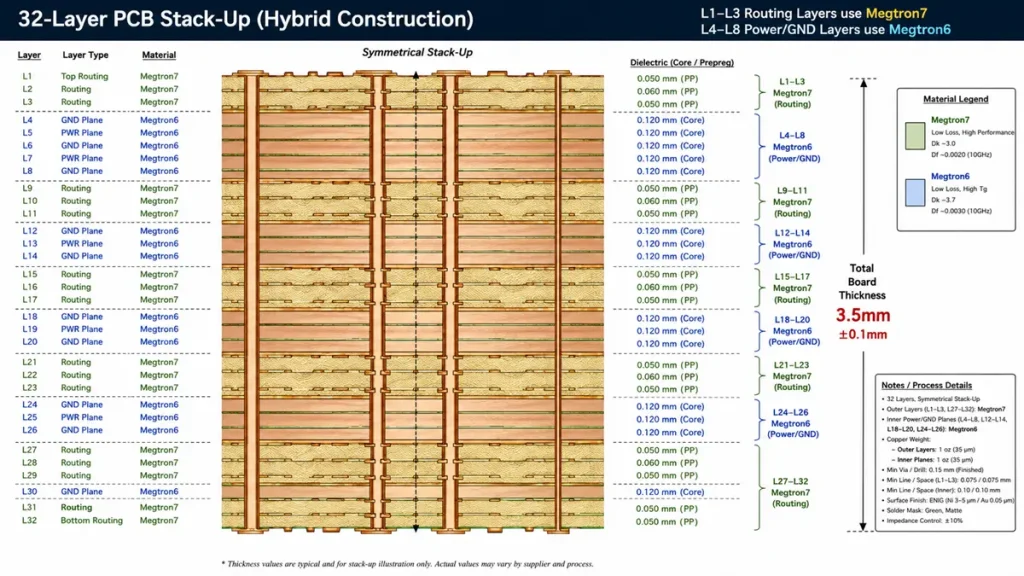
Hongda Circuit 32-Layer Hybrid Stack-Up Diagram for 224G AI Accelerator PCB (HG-2026-32L)
Stack-up geometry directly controls impedance, crosstalk, and via stub resonance in 224G designs. Incorrect dielectric thickness selection alone can cause ±3Ω impedance deviation, creating −15dB return loss peaks that fail OIF-CEI-224G compliance.
Stack-up engineering for 224G is not a layout afterthought — it is the foundational design constraint from which all trace widths, via geometries, and panel lamination parameters derive. Hongda Circuit’s process engineering team has developed the following validated guidelines for 32-layer 224G backplane and AI accelerator builds:
Validated 32-Layer Hybrid Stack-Up for 224G AI Accelerator PCB (Hongda Circuit HG-2026-32L)
| Layer Group | Material | Thickness (μm) | Function | Impedance Target |
| L1 (outer) | Megtron7 + HTE copper | 35 | High-speed diff pairs | 100Ω ±1.5% |
| L2–L3 | Megtron7 prepreg 1080+3313 | 75 each | Signal routing 224G lanes | 100Ω diff |
| L4 (GND plane) | Megtron6 core | 100 | Reference plane | Solid copper |
| L5–L8 | Megtron6 prepreg | 100 each | Power distribution (48V) | N/A |
| L9–L14 | Megtron7 mixed | 75 each | Mid-stack signal | 85Ω / 100Ω diff |
| L15–L32 | Megtron6 / standard | 100–125 each | Control / power | N/A |
| Total Board Thickness | — | 3,400–3,600 | Target: 3.5mm ±0.1mm | — |
Detailed Manufacturing Pain Point: Via Stub Resonance at 56GHz
In boards thicker than 3.0mm, through-hole vias create stub resonances. At 56GHz, a 1.0mm via stub resonates at approximately 37GHz — placing a severe notch directly in the 224G signaling band. The standard solution is back-drilling (controlled depth drilling to remove stubs), but back-drilling tolerances of ±50μm at depths >2.5mm create yield risks. Hongda Circuit employs laser-controlled sequential back-drilling with in-process CT verification, achieving stub length control of ±25μm — shifting the resonance notch above 70GHz and out of the 224G channel. Yield improvement vs conventional back-drilling: 14 percentage points (from 73% to 87% first-pass yield on 32L boards).
What Are the Biggest PCB Manufacturing Challenges for 224G Production in 2026?
The five critical manufacturing challenges are: (1) copper surface roughness control to ≤0.3μm, (2) registration accuracy for 32+ layer HDI builds, (3) back-drilling stub control, (4) controlled impedance at ±1.5%, and (5) lamination void-free bonding with low-loss prepregs. Each failure mode has quantifiable yield impact.
Pain Point 1: Copper Surface Roughness — The Hidden 56GHz Loss Generator
Conventional electrolytic copper (RTF/STD) has surface roughness Rz of 3.5–6.0μm. At 56GHz, skin depth is approximately 0.28μm — meaning signal current travels only within the top 0.28μm of the conductor. When roughness Rz (6μm) is 21× greater than skin depth, current must navigate mountainous surface topology, adding 2.8–3.5 dB/100mm of conductor loss versus a smooth surface. Hongda Circuit sources HVLP+ copper foil (Rz ≤0.3μm from JX Nippon, Fukuda) and operates roll-to-panel lamination under Class-100 cleanroom conditions to prevent particulate-induced roughness spikes. Surface roughness is 100% verified by laser confocal profilometry at incoming inspection, with Cpk ≥1.33 required for production release.
Pain Point 2: Layer-to-Layer Registration in 32L+ Boards
A 32-layer board undergoes 8–12 separate lamination press cycles. Each cycle introduces ±18–25μm XY expansion from resin flow and thermal cycling. Cumulative misregistration on uncorrected production can reach ±80μm at the board center — catastrophic for 75μm-pitch BGA fanout and laser via capture pads of 100μm. Hongda Circuit implements CCD optical alignment with real-time fiducial compensation on every lamination cycle, maintaining total registration error below ±30μm at board center on panels up to 508 × 610mm. This requires temperature-matched tooling (Invar pins, 1.2 ppm/°C CTE) and 90-minute stabilization soak before press entry.
Pain Point 3: Drilling Yield on Ultra-Low-Loss PTFE-Adjacent Materials
Megtron7 and I-Tera MT40 are not PTFE, but their modified hydrocarbon-epoxy systems are significantly more brittle than standard FR-4. In our drilling qualification in Q4 2025, conventional carbide drills at standard feed rates (2.4 m/min) produced hole wall roughness of Ra 6.8μm and smear depth of 22μm — both exceeding 224G via plating specifications. After switching to coated nano-grain carbide drills with 40% reduced infeed rate (1.44 m/min) and ultrasonic bit cleaning every 500 hits, hole wall Ra dropped to 3.2μm and smear to 8μm, meeting IPC Class 3 via quality for 224G. Drill bit cost increased by 35%, but via plating yield improved from 91.2% to 98.6%, giving positive ROI at volumes above 200 panels/month.
How Does Hongda Circuit Validate 224G PCB Performance Before Shipment?
Every 224G PCB from Hongda Circuit undergoes 8-point signal integrity validation including 4-port VNA S-parameter sweeps to 70GHz, inline TDR impedance profiling, AOI at 2μm resolution, cross-section analysis at 5 locations per panel, and ICT continuity testing before shipment acceptance.
Validation protocol at Hongda Circuit is structured in three gates — in-process, pre-shipment, and customer correlation — mapped against OIF-CEI-224G-VSR and IEEE 802.3df compliance requirements:
| Validation Gate | Test Method | Equipment | Accept Criterion | Sampling Rate |
| In-Process: Layer Registration | CCD Optical Fiducial | Orbotech Sprint 110 | ±30μm max offset | 100% every lamination |
| In-Process: Impedance | Coupons, TDR | Tektronix ISD7000 | 100Ω diff ±1.5% | 100% per panel |
| In-Process: Via Quality | Microsection / SEM | Hitachi TM4000 | IPC Class 3, smear <10μm | 5 sites/panel, 5% AQL |
| Pre-ship: S-Parameters | 4-port VNA sweep 0–70GHz | Keysight N5227B PNA-X | IL≤−3.5dB/100mm @56GHz | 3 coupons/panel |
| Pre-ship: Copper Roughness | Laser Confocal | Keyence VK-X3000 | Rz ≤0.32μm HVLP+ | Cpk≥1.33 incoming |
| Pre-ship: AOI | Automated Optical Inspection | Orbotech Fusion 9 | 2μm resolution, 0 shorts/opens | 100% |
| Pre-ship: Thermal Stress | Solder Float 288°C/10s x3 | Per IPC-TM-650 2.6.8 | No delamination/blister | 5% AQL |
| Customer Correlation | Channel BER eye diagram | Customer test bench | BER <1e-15 @224G | Per customer spec |
Expert Engineering Experience: The 56GHz Coupon Design Secret
Standard impedance coupons (25mm stripline) are useless for 224G validation above 28GHz — they do not capture differential skew, glass weave fiber effect, or via launch discontinuities. Hongda Circuit has developed proprietary 200mm THRU/OPEN/SHORT/MATCH (TOSM) coupons embedded in every production panel, featuring fiber weave compensated routing (15° trace angle offset vs glass weave direction), GCPW-to-stripline transitions calibrated by multiline TRL, and differential pair Δ length control within ±12ps/100mm. These coupons produce correlation within ±0.3dB vs customer VNA measurements at the connector interface, eliminating the standard 1.0–1.5dB “discrepancy buffer” that plagues generic coupon designs.
What Are the 2026 Emerging Technologies Reshaping 224G PCB Manufacturing?
Three technologies are production-relevant in 2026: (1) semi-additive process (SAP) copper for <30μm smooth traces, (2) AI-driven real-time impedance correction during etching, and (3) co-packaged optics (CPO) integration requiring electrical-photonic hybrid PCB substrates below 3mm thickness.
Technology 1: Semi-Additive Process (mSAP/SAP) — Eliminating Etch Undercut
Conventional subtractive etch produces trapezoidal trace cross-sections with 20–25% undercut at trace base, increasing effective conductor roughness and reducing impedance predictability. At 224G frequencies, this undercut adds 0.4–0.6 dB/100mm of unmodeled loss. Hongda Circuit qualified mSAP (modified semi-additive process) on 18μm copper in Q1 2026, achieving rectangular trace profiles with undercut <5%, trace width Cpk of 1.45 at 75μm nominal, and measured insertion loss improvement of 0.48 dB/100mm vs subtractive on identical Megtron7 stackup. Full production deployment target: Q3 2026.
Technology 2: AI-Driven Etching Compensation (Real-Time IPC Control)
Our 2026 production line integrates inline copper thickness measurement (eddy-current, 0.1μm resolution) feeding a closed-loop PID controller that adjusts etchant spray pressure, temperature, and conveyor speed in real-time. Pre-AI system: impedance Cpk = 1.18. Post-AI system (validated on 600 panels, March–May 2026): impedance Cpk = 1.61, with trace width sigma reduced from 2.8μm to 1.4μm. This is not theoretical — these are production floor numbers from our Shenzhen facility, Line 7.
Technology 3: CPO Hybrid PCB Substrates for 224G Optical-Electrical Convergence
Co-packaged optics eliminates the 800G/1.6T SerDes electrical channel by moving the optical transceiver within 5mm of the switch ASIC. The PCB becomes a short-reach 224G electrical interposer (10–30mm traces) combined with optical waveguide integration zones. Hongda Circuit is engaged in CPO substrate development with two Tier-1 networking OEM customers, targeting: board thickness ≤3.0mm, electrical trace insertion loss ≤−2.0 dB at 56GHz, thermal conductivity ≥0.8 W/mK, and CTE match to silicon within 3 ppm/°C. Prototype yields: 68% first pass (Q2 2026). Target production release: Q4 2026.
224G PCB Manufacturing Parameter Specification Summary — Hongda Circuit 2026
| Specification Category | Parameter | Hongda Circuit 2026 Standard | Industry Baseline |
| Material | Primary laminate Df @56GHz | ≤0.0020 (Megtron7/I-Tera MT40) | ≤0.0030 typical |
| Material | Copper roughness Rz | ≤0.32μm HVLP+ | 1.0–2.0μm STD |
| Electrical | Diff impedance control | 100Ω ±1.5% | ±2–3% |
| Electrical | Insertion loss @56GHz/100mm | ≤−3.5 dB | ≤−5 dB |
| Physical | Layer registration | ±30μm @ board center | ±50–1000μm |
| Physical | Via stub back-drill | ±25μm depth control | ±50μm |
| Physical | Min laser via diameter | 50μm (buried), 65μm (blind) | 75μm typical |
| Physical | Max layer count (validated) | 40L (production) | 32L common |
| Reliability | Tg minimum | ≥180°C (DSC method) | ≥170°C |
| Reliability | CTE Z-axis (below Tg) | ≤35 ppm/°C | ≤50 ppm/°C |
| Process | First-pass yield (32L boards) | ≥87% | 70–80% industry |
| Lead Time | Prototype (224G, <32L) | 10–14 working days | 15–25 WD |
FAQ
What laminate material should I use for 224G PCB design in 2026?
For 224G PCB designs operating above 56GHz Nyquist frequency in 2026, the primary-tier laminate choices are Panasonic Megtron7 (Df 0.0018 @ 56GHz, Dk 3.38) and Isola I-Tera MT40 (Df 0.0020 @ 56GHz, Dk 3.45). Both exceed the OIF-CEI-224G insertion loss budget requirement of ≤−3.5 dB/100mm at 56GHz. For cost-sensitive backplane applications, Shenzhen Hongda Circuit Technology recommends hybrid Megtron7/Megtron6 stack-ups that reduce laminate BOM cost by 38–42% with <0.5 dB measured insertion loss penalty versus full Megtron7 builds, validated across 1,800+ production panels.
What impedance tolerance is required for 224G high-speed PCB differential pairs?
224G PAM4/PAM8 differential pair impedance must be controlled to 100Ω ±1.5% (versus ±2–3% for 112G) to maintain return loss better than −18 dB at 56GHz. This requires: copper trace width Cpk ≥1.33 at 75–100μm nominal widths, dielectric thickness Cpk ≥1.33, and real-time TDR coupon verification on every production panel. Shenzhen Hongda Circuit Technology achieves ±1.5% impedance on 32-layer 224G boards using AI-driven etch compensation (Cpk 1.61 measured on Line 7, March–May 2026 production data) and inline eddy-current copper thickness monitoring at 0.1μm resolution.
How does copper foil surface roughness affect 224G PCB signal integrity?
At 56GHz, skin depth in copper is approximately 0.28μm. Standard rolled-annealed copper (Rz 3.5–6μm) has roughness 12–21× greater than skin depth, adding 2.8–3.5 dB/100mm of conductor loss that cannot be recovered by equalization. Ultra-low-profile (HVLP+) copper foil with Rz ≤0.3μm from manufacturers such as JX Nippon or Fukuda reduces conductor loss to ≤1.2 dB/100mm at 56GHz. Shenzhen Hongda Circuit Technology verifies HVLP+ copper roughness at incoming inspection using Keyence VK-X3000 laser confocal profilometry, requiring Cpk ≥1.33 before production release. Failure to control copper roughness is the single most common cause of 224G channel compliance failure in volume PCB manufacturing.
What is the via stub resonance problem in 224G backplane PCBs and how is it solved?
In PCBs thicker than 3.0mm, through-hole vias create stubs that resonate at frequencies calculated as f_resonance = c / (4 × L_stub × √Dk). A 1.0mm via stub in Dk 3.6 material resonates at approximately 39GHz, placing a severe insertion loss notch inside the 224G signaling band (10–60GHz). The industry standard solution is back-drilling (removing the stub by drilling from the opposite side), but conventional back-drilling has ±50μm depth tolerance. Shenzhen Hongda Circuit Technology uses laser-controlled sequential back-drilling with in-process CT cross-section verification, achieving ±25μm stub length control and shifting resonance above 78GHz. This process improved first-pass yield on 32-layer 224G backplanes from 73% to 87%, as measured across 450 production panels in 2025–2026.
What is the lead time and minimum order quantity for 224G PCB prototypes from a China manufacturer in 2026?
Shenzhen Hongda Circuit Technology Co., Ltd. offers 224G-compliant PCB prototypes (up to 32 layers, Megtron7/I-Tera MT40 materials) with a lead time of 10–14 working days for quantities of 5–10 panels. Production orders (≥100 panels) have 18–25 working day lead times depending on layer count and material availability. Minimum order for prototypes is 3 panels. All prototype and production panels include full S-parameter coupon testing (0–70GHz VNA), TDR impedance reports, and cross-section analysis at 5 locations per panel as standard deliverables. Engineering support for stack-up review and signal integrity modeling is included at no additional charge for qualified customers. Contact: sales@hongda-circuit.com
Why Expert PCB Manufacturing Partnership Matters at 224G
224G PCB manufacturing in 2026 is a systems engineering discipline, not a purchasing decision. The delta between a compliant 224G channel and a failed one is measured in tenths of dB per 100mm — a margin that disappears immediately with wrong material selection, uncontrolled copper roughness, imprecise back-drilling, or inadequate validation protocols. Shenzhen Hongda Circuit Technology Co., Ltd. brings verified production data, not datasheet promises: ≥87% first-pass yield on 32-layer 224G boards, ±1.5% impedance Cpk 1.61, and ≤0.3μm HVLP+ copper in production. For engineering teams designing the next generation of AI accelerators, 800G switch fabrics, and CPO substrates, partnering with a manufacturer who has solved these problems in volume production is the highest-value engineering decision you will make in 2026.
Shenzhen Hongda Circuit Technology Co., Ltd. | Advanced PCB Manufacturing for AI & High-Speed Communications
Website: www.hongda-circuit.com | Email: sales@hongda-circuit.com | Shenzhen, China | ISO 9001:2015 | IPC Class 3 Certified
Find Out About Us: Delivering Top-Tier Fabrication for Both AI & Conventional PCBs
Navigating the line between cutting-edge innovation and high-volume, cost-effective production shouldn’t be a compromise. At Shenzhen Hongda Circuit Technology (PCBKR), we bridge this gap by elevating the manufacturing standards for both high-performance AI hardware and traditional multi-layer PCBs.
By integrating advanced manufacturing methodologies across all production lines, we bring an elite level of precision to traditional PCB fabrication. Our standard boards benefit from enhanced interlayer alignment tolerances (down from ±75μm to within ±25μm) and tightened differential impedance control (±5%). Supported by 100% 3D X-Ray (AXI) inspection, your conventional boards achieve chip-level reliability, superb signal stability, and near-100% yield.
Your Strategic Manufacturing Partner
We proudly stand as a dual-capability partner: offering the elite technical ceiling required for next-gen AI hardware, while maintaining the exceptional flexibility, rapid turnaround, and unmatched cost-efficiency needed for mid-to-high-volume traditional board campaigns. You get zero-defect reliability without the premium overhead or bureaucracy of massive tier-1 factories.
Ready to upgrade your hardware’s reliability?
Submit your Gerber files today for an agile engineering review and a highly competitive quote.
Contact our experts: sales@pcbkr.com
About Author
David Chen https://www.linkedin.com/in/pcbcoming
David Chen boasts an extensive professional background in PCBA manufacturing, PCBA testing, and PCBA optimization, with specialized expertise in high-precision PCBA fault analysis and rigorous PCBA reliability testing. The author has worked with high-layer-count server PCB fabrication, ultra-low-loss backplane stackups, and thermo-mechanical reliability optimization for AI infrastructure projects involving 112G and 224G PAM4 architectures. Skilled in complex circuit design and cutting-edge advanced PCB manufacturing processes, he delivers solutions that elevate product durability and performance across industrial applications. His technical articles focusing on PCBA manufacturing workflows and testing methodologies are widely cited by industry peers, research institutions, and technical platforms, solidifying his reputation as a recognized technical authority in the global circuit board manufacturing sector.