Cost Analysis: 4-Layer Heavy Copper PCB for Power Supply Units (2026 Engineering & Procurement Guide)
Anyone sourcing a heavy copper PCB 4 layer power supply cost per board quickly discovers that pricing is rarely a single number. It moves with copper weight, laminate grade, stack-up complexity, panel yield, and hole geometry — and it moves further once 2026-era manufacturing methods such as pulse plating and AI-assisted DFM enter the picture. This guide breaks the cost down the way a fabrication engineer would, so buyers and design engineers can request a quote that is accurate on the first pass rather than the third.
At Shenzhen Hongda Circuit Technology Co., Ltd., we build 4-layer and multilayer heavy copper boards for power supply units, inverters, motor drives, and industrial power modules every day. This article shares how we actually price a board — not a generic price list, but the logic behind it.
1. Why Cost-per-Board Clarity Matters for Power PCB Sourcing
Power electronics teams rarely buy a “PCB” — they buy current-carrying capacity, thermal margin, and long-term reliability packaged into a board. That changes how cost should be evaluated. A board that looks cheaper per square inch can end up more expensive once copper thickness, layer count, and finish are matched to the electrical load.
This page is written for two audiences with different priorities but the same underlying question:
- Procurement teams comparing supplier quotes for a 4-layer heavy copper power PCB and needing to understand what drives price variance between vendors.
- Design and power engineers who need to estimate heavy copper PCB cost early enough to influence stack-up and copper weight decisions before tooling starts.
Typical applications driving this search include power supply modules, industrial power converters, solar inverter boards, motor controllers, and high-current busbar replacements — all cases where a 4-layer heavy copper stack-up balances cost against current capacity better than a 2-layer or ultra-thick single-layer design.
2. What Makes Up the Cost Per Board on a 4-Layer Heavy Copper Power PCB
2.1 The Core Components of Cost Per Board
Every quotation, regardless of supplier, is really assembling three cost blocks:
- Material cost — copper foil, laminate (core and prepreg), and surface finish chemistry.
- Process cost — plating time, etching cycles, lamination pressure profiles, drilling, and inspection labor tied to heavy copper handling.
- Engineering and yield cost — DFM review, tooling, panel utilization, and the scrap rate inherent to thick-copper etching tolerances.
2.2 Raw Material Cost vs. Manufacturing Process Cost
For a standard 1oz FR-4 board, material typically dominates the price. Once copper weight climbs to 4oz or 6oz, that ratio flips: process cost — extended plating cycles, differential etching, and thicker resin fill — becomes the larger share of the invoice. This is the single most common misunderstanding buyers have when comparing a heavy copper PCB quote against a standard PCB quote line by line.
2.3 Engineering and Customization Factors That Move the Price
Custom impedance control, non-standard copper distribution between layers, embedded copper coins for localized heat sinking, and tight aspect-ratio vias all add engineering review time before the panel ever reaches production. Suppliers with in-house DFM automation — including AI-assisted stack-up simulation, which has become standard practice among leading heavy copper fabricators in 2026 — can absorb much of this review time without passing it fully into the quote, which is one reason quotes vary so widely between vendors for what looks like an identical spec sheet.
3. Heavy Copper PCB Cost Drivers: A Layer-by-Layer Breakdown
3.1 Copper Weight and Its Effect on Heavy Copper PCB Pricing (4oz vs 6oz)
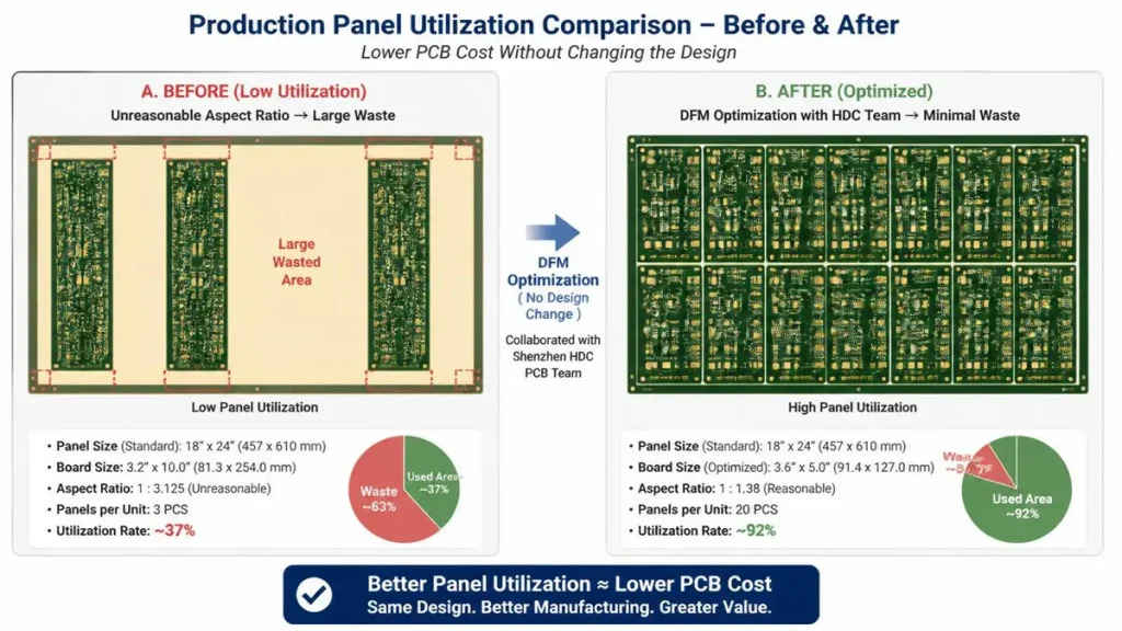
Comparison of 4-layer PCB panel utilization[cite: 1]. Left (A): Poor layout with 63% wasted area due to unreasonable aspect ratio[cite: 1]. Right (B): Optimized 92% utilization achieved via HDC DFM team without changing the original board design
Copper weight is the single biggest lever on a 4 layer heavy copper PCB price.
- 4oz copper is the common entry point for “heavy copper” classification and suits most power supply and industrial control applications requiring higher current handling than standard 1oz–2oz boards.
- 6oz and above increases current-carrying capacity substantially but requires longer plating cycles, wider etch compensation, and tighter process control to hold trace geometry — all of which raise per-panel cost.
The trade-off engineers should evaluate isn’t just “more copper equals more cost.” It’s whether the added copper weight removes the need for external heat sinks or parallel traces elsewhere in the design — often the real cost savings shows up at the system level, not the board level.
3.2 Material Selection: Standard FR-4 vs High Tg / High CTI Laminates for Power PCBs
Power supply boards run hotter and carry higher current density than typical digital PCBs, so laminate selection is a reliability decision as much as a cost one.
- Standard FR-4 works for moderate thermal loads and cost-sensitive designs.
- High Tg (≥170°C) and high CTI laminates are increasingly specified for power PCBs operating near enclosure limits or in automotive and renewable-energy environments, where sustained thermal cycling and creepage/clearance requirements are stricter.
Material cost as a share of the total quote typically runs higher on heavy copper boards than on standard boards, simply because thicker copper needs thicker, more thermally stable resin systems to stay flat and reliable through reflow.
3.3 4-Layer Stack-up Design and Its Impact on Manufacturing Cost
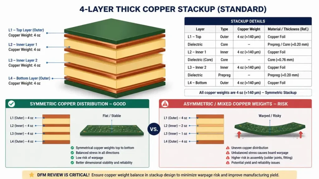
4-Layer thick copper stackup design analysis[cite: 1]. A symmetric copper distribution (left) ensures a flat, stable board[cite: 1]. An asymmetric stackup with mixed copper weights (right) significantly increases warpage risk, highlighting why an experienced DFM review is critical to controlling manufacturing cost and yield
A 4-layer heavy copper power PCB stack-up usually separates power planes from signal/control layers. How copper is distributed between outer and inner layers changes both electrical performance and lamination difficulty:
- Symmetric copper distribution reduces warpage risk during lamination.
- Mixed copper weights within one stack-up (e.g., 4oz power layers with 1oz signal layers) require more precise pressure and cure-cycle control, which adds process cost.
- Stack-up complexity is one of the first things an experienced fabricator’s DFM team will flag, since it directly affects both yield and price.
3.4 Panel Utilization: The Overlooked Lever in Heavy Copper PCB Cost Per Board
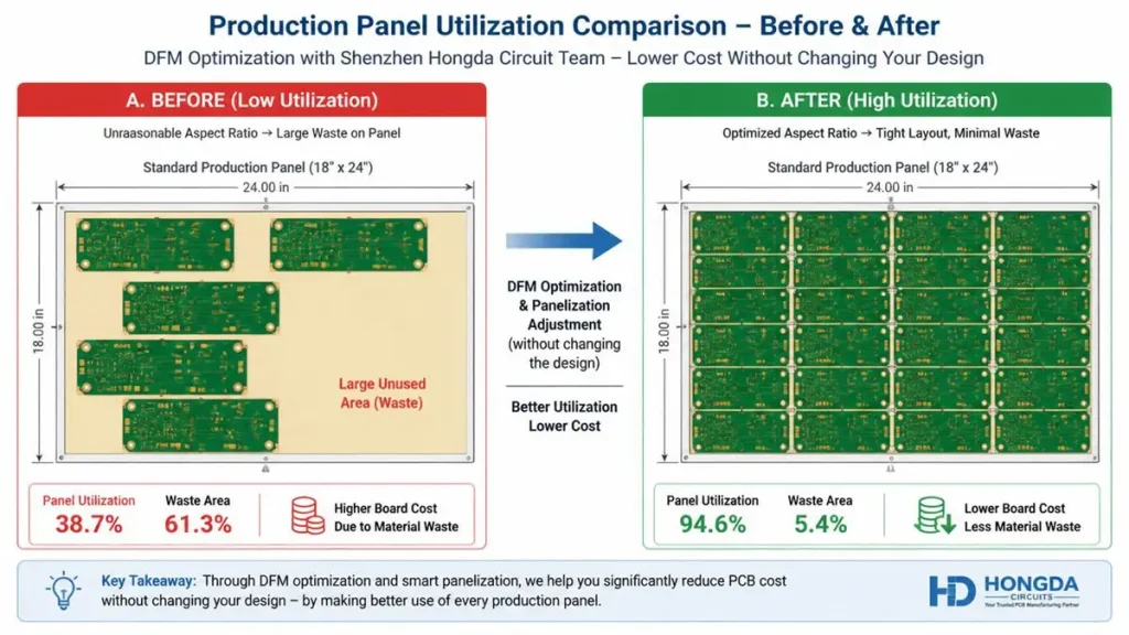
How DFM optimization improves production panel utilization[cite: 1]. Left (A) shows 61.3% material waste due to an unreasonable aspect ratio. Right (B) shows a tight layout with 94.6% utilization achieved by cooperating with the Shenzhen Hongda Circuit engineering team—significantly reducing the final cost per board without changing the original design.
Panel utilization — how efficiently individual boards are arranged (single-image vs. multi-image panelization) — has an outsized effect on the per-board price, even though it rarely appears explicitly on a quote.
- Boards with awkward aspect ratios or large keep-out zones waste panel area.
- Improving utilization through smarter panelization, without changing the board design itself, can lower cost per unit meaningfully — something a good supplier will proactively suggest rather than quoting the design as submitted.
3.5 Hole Structure and Drilling Difficulty in Thick Copper Boards
Heavy copper introduces drilling and plating challenges that don’t exist on standard boards:
- Higher aspect-ratio vias are harder to plate evenly through thick copper layers.
- Larger via count on power planes increases both drill time and copper-fill volume during electroplating.
- Process yield on thick-copper drilling and plating directly affects the price a fabricator can offer — suppliers with mature thick-copper plating lines can hold tighter tolerances at a lower reject rate, which shows up as a more competitive quote.
3.6 Surface Finish Options and Their Cost Difference on Heavy Copper Boards
Common finishes — HASL, lead-free HASL, ENIG, and immersion silver — behave differently on heavy copper boards because the underlying copper topology is less uniform than on thin-copper boards.
- HASL remains the most economical option for many power applications where fine-pitch components aren’t present.
- ENIG is typically specified when the board also carries surface-mount control circuitry alongside the heavy copper power section, since it offers a flatter, more solderable finish for fine-pitch parts.
Finish selection should match the actual component mix on the board — over-specifying ENIG on a purely power-plane board is a common source of avoidable cost.
4. Typical Price Ranges for a 4-Layer Heavy Copper Power PCB (Engineering Perspective)
Exact pricing depends on volume, copper weight, and finish, but a few patterns hold consistently across the industry:
- 4oz vs 6oz copper: moving from 4oz to 6oz typically adds a noticeable percentage premium per panel, driven mainly by plating cycle time rather than raw copper volume alone.
- Small-batch vs. mid-volume runs: unit price drops meaningfully once a project moves from prototype quantities into mid-volume production, largely because tooling and engineering cost amortize across more boards.
- Customization: non-standard copper distribution, tight tolerances, or specialty laminates shift a project from “standard heavy copper PCB pricing” toward a custom quote requiring full DFM review.
Because these ranges vary by design specifics, the most reliable way to get an accurate number is a real quote against your Gerber and stack-up files rather than a published price table.
5. How to Reduce the Unit Price of a 4-Layer Heavy Copper Power Board
Buyers and design teams have more influence over final cost than most quotes suggest. In practice, the highest-impact levers are:
- Balance copper weight against actual current requirements — don’t default to the heaviest copper available if 4oz meets the thermal and current-carrying target.
- Improve panel utilization by working with your fabricator’s panelization team before finalizing board outline dimensions.
- Simplify stack-up complexity where possible — fewer copper-weight transitions between layers reduces lamination risk and cost.
- Submit complete engineering data up front — Gerber files, IPC netlist, full stack-up definition, and impedance requirements at the RFQ stage prevent costly re-quotes and production delays later.
6. 2026 Manufacturing Technologies Shaping Heavy Copper PCB Cost and Quality
Heavy copper fabrication has moved forward meaningfully over the past few years, and the manufacturing methods a supplier uses now directly affect both price and reliability:
- Pulse and reverse-pulse plating deliver more uniform copper distribution across thick layers, reducing scrap from uneven plating — a direct contributor to more stable heavy copper PCB pricing.
- AI-assisted DFM and stack-up simulation catch impedance, warpage, and lamination-risk issues before tooling starts, cutting the engineering iteration time that used to be baked into custom quotes.
- Sequential lamination enables hybrid stack-ups that combine heavy copper power layers with finer-pitch signal layers in a single 4-layer board, avoiding the cost of splitting a design across two separate boards.
- Copper-coin and copper-inlay embedding provide localized heat spreading for high-power components without resorting to full 6oz+ copper across the entire board — often a more cost-effective thermal solution.
- AI-enhanced automated optical inspection (AOI) improves defect detection on thick-copper etch profiles, supporting tighter tolerances at production volume without a proportional increase in rejects.
Shenzhen Hongda Circuit Technology Co., Ltd. has integrated these process upgrades into our heavy copper production lines specifically to keep 4-layer power PCB pricing predictable as copper weight and design complexity increase.
7. Get an Accurate Heavy Copper PCB Cost Per Board Quote
7.1 What to Submit for a Precise Quotation
To receive a quote that won’t change once engineering review begins, prepare:
- Gerber files (RS-274X or ODB++)
- Copper weight per layer
- Laminate/material specification (or performance requirements if material is open)
- Order quantity and expected reorder volume
- Any impedance-controlled nets or special tolerances
7.2 Quote Response Time
Our engineering team typically returns a reviewed cost per board quotation within 3–6 hours of receiving complete files, including flagged DFM concerns if any exist — so you’re pricing the board you can actually build, not the one on paper.
7.3 Why Buyers Choose Shenzhen Hongda Circuit Technology Co., Ltd.
- Dedicated heavy copper production capability from 3oz through 10oz+
- In-house DFM and stack-up engineering support at the quoting stage
- Transparent cost breakdowns rather than flat per-board pricing
- Manufacturing processes built around 2026-current plating and inspection standards
8. Request Your Custom Cost-Per-Board Analysis
If you’re comparing suppliers for a 4-layer heavy copper power PCB, the fastest way to get a number you can actually plan around is a direct quote against your own files.
Submit Your Gerber Files for a full engineering-reviewed quotation, including a detailed cost-per-board breakdown and DFM feedback specific to your stack-up and copper weight.
FAQ
How much does a 4-layer heavy copper PCB cost per board?
Cost per board depends primarily on copper weight, laminate grade, stack-up complexity, and order volume. A 4oz 4-layer heavy copper power PCB is generally more economical than a 6oz+ equivalent because of shorter plating cycles and simpler etch compensation. The only reliable figure comes from a quote run against your actual Gerber files and stack-up.
What’s the difference between a standard PCB supplier and a heavy copper PCB manufacturer?
Heavy copper fabrication requires plating equipment, etching control, and lamination pressure profiles capable of handling 3oz copper and above without compromising trace geometry or reliability. Not every PCB shop runs production-grade heavy copper lines, so it’s worth confirming a supplier’s actual thick-copper capability — not just their advertised layer count — before requesting a quote.
How do I compare heavy copper PCB quotes from different suppliers fairly?
Line up quotes by copper weight, laminate type, surface finish, and panel utilization rather than by the bottom-line number alone. Two quotes for the “same” board can differ significantly if one supplier assumes a lower-grade laminate or a less efficient panelization than the other.
How long does it take to get a quote for a custom heavy copper power PCB?
With complete engineering files — Gerber, stack-up, copper weight, and quantity — most experienced heavy copper fabricators, including Shenzhen Hongda Circuit Technology Co., Ltd., can return a reviewed quote within a few hours to one business day. Incomplete files typically add a review cycle before pricing can be finalized.
What information does a supplier need to give an accurate heavy copper PCB cost estimate?
At minimum: Gerber files, copper weight per layer, base material specification or performance requirements, order quantity, and any impedance or tolerance requirements. Providing this up front avoids re-quoting after DFM review and shortens the path from RFQ to production.
About Author
David Chen https://www.linkedin.com/in/pcbcoming
David Chen boasts an extensive professional background in PCBA manufacturing, PCBA testing, and PCBA optimization, with specialized expertise in high-precision PCBA fault analysis and rigorous PCBA reliability testing. The author has worked with high-layer-count server PCB fabrication, ultra-low-loss backplane stackups, and thermo-mechanical reliability optimization for AI infrastructure projects involving 112G and 224G PAM4 architectures. Skilled in complex circuit design and cutting-edge advanced PCB manufacturing processes, he delivers solutions that elevate product durability and performance across industrial applications. His technical articles focusing on PCBA manufacturing workflows and testing methodologies are widely cited by industry peers, research institutions, and technical platforms, solidifying his reputation as a recognized technical authority in the global circuit board manufacturing sector.