How to Choose a Reliable Heavy Copper PCB Manufacturer forHigh-Power Applications in 2026
Selecting a heavy copper PCB manufacturer is rarely a simple sourcing decision. For engineers designing power modules, inverters, EV drive units, or energy storage systems, the board itself is part of the power path — and a poor fabrication choice shows up later as thermal failures, delamination, or missed production deadlines. Two forces make this decision more consequential in 2026 than it was even three years ago: high-power electronics are pushing copper weights and current densities higher, and PCB manufacturing technology itself has advanced enough that not every supplier claiming “heavy copper” capability can actually deliver it at scale.
This guide walks through why heavy copper construction matters for high-power designs, how the global supplier landscape is shifting, which qualifications actually separate capable factories from the rest, and a practical framework for vetting a partner before you commit a production order. Shenzhen Hongda Circuit Technology Co., Ltd. shares its own factory capabilities throughout as a reference point for what a mature heavy copper PCB manufacturer should be able to demonstrate.
Why Heavy Copper PCBs Are Critical for High-Power Applications
A heavy copper PCB is generally defined as a board carrying copper weight of 3 oz or more per layer, with capable manufacturers extending that to 10 oz or beyond on select layers. The extra copper isn’t cosmetic — it directly changes how a board behaves electrically and thermally.
In power supplies, inverters, frequency converters, and EV battery management systems, conductors carry sustained high currents. Thin standard copper traces under that load generate excess resistive heating and voltage drop, both of which degrade efficiency and shorten component life. Increasing copper thickness lowers trace resistance, so the same current produces less heat and less loss. That extra copper mass also acts as a passive heat spreader, pulling heat away from hot components and distributing it across the board rather than letting it concentrate at a single point.
For applications such as industrial power supplies, solar and wind inverters, EV charging systems, welding equipment, and battery energy storage systems, this translates into measurable gains in reliability and service life — which is exactly why heavy copper PCB manufacturers have become a specialized, closely scrutinized category of supplier rather than a generic PCB vendor offering a thicker option.
Global Landscape of Heavy Copper PCB Manufacturers: Why China Leads
The Shift Toward Chinese Heavy Copper PCB Manufacturers
Heavy copper PCB capacity exists across North America, Europe, and Asia, but the center of gravity has moved decisively toward China over the past decade. Buyers in the United States, Germany, and other established industrial markets increasingly qualify a Chinese heavy copper PCB manufacturer as either their primary supplier or a strategic backup source, driven by production scale, mature process control, and cost structures that Western fabs struggle to match on comparable order volumes.
This isn’t simply about lower labor cost. Chinese PCB clusters — particularly in the Pearl River Delta — have built up dense supply chains for copper foil, laminate, and specialty surface finishes, which shortens lead times and reduces the material bottlenecks that often slow heavy copper production elsewhere.
Core Competencies of Leading Heavy Copper PCB Manufacturers in China
The manufacturers that have earned international qualification typically share a specific set of capabilities:
- Large-format panel handling with high-layer-count builds that support complex power and control circuitry on a single board.
- Multi-ounce copper processing, often extending well beyond the 3–6 oz range that many general-purpose fabs treat as their ceiling.
- Stepped copper foil lamination, allowing a single board to carry different copper weights in different zones — heavy copper in the power section, standard copper in the signal section.
- Certifications relevant to regulated industries, including IATF16949 for automotive programs, ISO9001 as a baseline quality system, and UL recognition for markets that require documented safety compliance.
For international buyers, the practical takeaway is that a well-vetted Chinese heavy copper PCB manufacturer can deliver automotive- and industrial-grade quality at a cost and lead time that supports both primary production and supply-chain diversification.
2026 PCB Manufacturing Technology Trends Shaping Heavy Copper Production
Heavy copper fabrication has benefited from broader advances in PCB manufacturing technology, and several developments are now standard practice among leading-edge factories rather than experimental capability.
Precision Stepped-Copper Lamination and Differential Etching
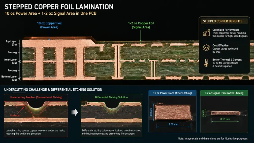
Cross-section view of a 10 oz power area integrated with a 1-2 oz signal area on a single PCB layer, showcasing the differential etching solution to eliminate undercutting.
Modern lamination presses and etching lines now hold tighter tolerances on stepped-copper boards, where a design calls for 10 oz copper in a power zone alongside 1–2 oz copper in a fine-pitch signal zone on the same layer. Improved differential etching control reduces the risk of trace undercutting on the heavy-copper side while preserving fine-line resolution on the signal side — a combination that was difficult to achieve reliably even five years ago.
AI-Assisted Process Control and Inspection
Automated optical inspection systems increasingly incorporate machine-learning models trained specifically to flag copper-thickness variation, resin voids, and lamination defects that are easy to miss on thick-copper boards using conventional inspection thresholds. This shifts defect detection earlier in the production line, which matters disproportionately for heavy copper work, where rework is costly and thermal cycling defects often only surface under load testing.
Embedded Copper Coin and Advanced Thermal Structures
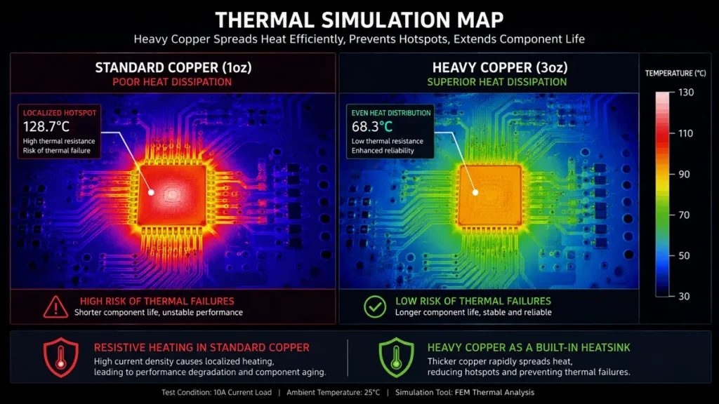
Thermal Simulation Map of Standard Copper vs. Heavy Copper PCB
For the highest-power designs, some manufacturers now embed solid copper coins or copper inlays directly into the board beneath high-heat components, supplementing heavy copper traces with a dedicated low-resistance thermal path. This is increasingly paired with resin or copper-paste via filling to eliminate air gaps that would otherwise limit heat transfer through the board stack.
Materials for High-Frequency, High-Power Convergence
As power electronics designs increasingly combine high current with switching frequencies in the hundreds of kilohertz to megahertz range, laminate suppliers have introduced high-Tg, low-loss materials that hold up under both heavy copper thermal cycling and higher-frequency signal integrity requirements. A capable heavy copper PCB manufacturer in 2026 should be able to advise on and stock these materials rather than defaulting to standard FR-4 for every build.
Halogen-Free and Lower-Emission Production
Environmental compliance has moved from a compliance checkbox to a standard specification, particularly for boards destined for the EU and other regulated markets. Halogen-free laminates, RoHS-compliant surface finishes, and lower-emission etching chemistries are now baseline expectations for factories serving automotive and energy-storage customers.
Together, these trends mean that “heavy copper capability” in 2026 is no longer just about how thick a factory can plate copper — it’s about whether the factory has integrated modern process control, materials, and thermal engineering into that capability.
Key Qualification Standards for Heavy Copper PCB Suppliers
Before evaluating any factory’s technical claims, buyers should confirm the certifications that indicate a supplier has the process discipline to back them up.
ISO9001 Quality Management System
ISO9001 is the baseline expectation for any serious PCB supplier. It confirms the factory operates under a documented quality management system with traceable process control — a minimum requirement, not a differentiator, but one that should never be missing.
IATF16949 Automotive-Grade Certification
For buyers sourcing boards for EV powertrains, battery management systems, or other automotive power electronics, IATF16949 certification is close to a hard requirement. It demonstrates the supplier’s quality system meets the specific traceability, defect-rate, and process-capability standards that automotive OEMs and Tier 1 suppliers demand.
UL Recognition and IPC Standards Compliance
UL certification addresses material and finished-board safety performance — flammability rating, thermal endurance, and electrical safety — and is particularly important for products shipping into the US and EU. Alongside UL, compliance with IPC standards such as IPC-A-600 (acceptability of printed boards) and IPC-6012 (qualification and performance for rigid printed boards) signals that the manufacturer’s inspection criteria align with internationally recognized benchmarks rather than an internal standard of unknown rigor.
Depending on the end application, buyers in medical or data-security-sensitive industries may also want to confirm ISO13485 or ISO27001 where relevant.
Shenzhen Hongda Circuit Technology’s Factory Capabilities for Heavy Copper PCBs
Shenzhen Hongda Circuit Technology Co., Ltd. publishes the following capability data for buyers evaluating a heavy copper PCB manufacturer for high-power programs. Figures reflect standard production capability; project-specific limits should always be confirmed during technical review.
| Capability | Specification |
|---|---|
| Copper thickness | 1 oz – 10 oz standard, higher on request |
| Stepped copper foil | Supported, mixed thickness on the same layer |
| Layer count | 1 – 26 layers |
| Board thickness | 0.2 mm – 6.0 mm |
| Maximum panel size | Large-format, up to meter-class boards |
| Special processes | HDI, resin plug, copper-paste plug, stepped holes, slot holes, thick gold plating |
| Surface finishes | ENIG, HASL, immersion tin, hard gold, electroless nickel palladium gold |
| Certifications | ISO9001, IATF16949, UL-recognized materials, IPC-A-600 / IPC-6012 compliant |
| Standard lead time | 10–15 business days |
| Expedited lead time | 5–7 business days for small-batch thick-copper orders |
Step-by-Step Guide to Choosing a Reliable Heavy Copper PCB Manufacturer
1. Define the project requirements precisely. Confirm application type (power supply, EV, energy storage), required copper thickness by zone, layer count, board dimensions, laminate type, and surface finish before contacting suppliers.
2. Build a shortlist of global heavy copper PCB manufacturers. Use industry referrals, trade shows, and search research to identify 3–5 candidates, giving particular weight to Chinese heavy copper PCB manufacturers given their combination of process maturity and cost efficiency.
3. Verify certifications directly. Request current ISO9001, IATF16949, and UL documentation rather than relying on website claims, and confirm the supplier’s IPC standard of reference.
4. Validate technical capability with evidence. Ask for coupon test boards or a small pilot run that demonstrates actual stepped-copper lamination, plating uniformity, and via-fill quality at the copper weight your design requires.
5. Assess capacity and delivery reliability. Compare standard and expedited lead times, monthly production capacity, and whether the factory can support multi-region delivery if your supply chain spans the US, Europe, and Asia.
6. Evaluate total cost, not just unit price. Request a full quotation including engineering fees, testing, and freight, and weigh that against quality consistency and delivery performance — the lowest unit price rarely produces the lowest total program cost on heavy copper builds.
7. Run a paid trial order before committing long-term volume. Place one or two small-batch orders, evaluate real-world quality and on-time delivery, and use that performance data — not the sales pitch — to decide on a long-term heavy copper PCB manufacturer relationship.
Request a Quote for Your Heavy Copper PCB Project
Shenzhen Hongda Circuit Technology Co., Ltd. supports high-oz copper builds, multilayer lamination, and the specialty processes covered above, backed by ISO9001, IATF16949, and UL-aligned quality systems for customers in the US, Europe, and beyond. To request a quote, submit the following:
- Project name and product category
- PCB specification: layer count, dimensions, copper thickness (oz), base material (e.g., FR-4, high-frequency laminate)
- Surface finish requirement
- Estimated order volume (prototype, small batch, or mass production)
- Target lead time
- Contact details: name, company, email, phone
- Supporting files if available: Gerber, BOM, specification sheet
Submit an RFQ and the engineering team typically responds within 24 hours with technical feedback and pricing. Email: pcb@pcbkr.com
Frequently Asked Questions
What copper thickness qualifies as “heavy copper” in PCB manufacturing?
Most of the industry defines heavy copper as 3 oz per square foot or above, with capable heavy copper PCB manufacturers able to process up to 10 oz or higher on select layers using stepped lamination techniques.
Why do buyers increasingly source from Chinese heavy copper PCB manufacturers?
Chinese suppliers have built dense, mature supply chains for copper foil and specialty laminates, along with the automotive and safety certifications international buyers require, which supports competitive pricing without sacrificing process consistency on multi-ounce copper builds.
Which certifications should a heavy copper PCB supplier hold for automotive or EV
projects?
IATF16949 is close to mandatory for automotive-grade programs, and should be paired with ISO9001 as a baseline quality system and UL recognition where the product ships into markets with formal safety compliance requirements.
How long does it typically take to produce heavy copper PCBs?
Standard heavy copper production commonly runs 10–15 business days, with some manufacturers offering expedited turnaround of 5–7 business days for smaller thick-copper batches.
What should a buyer request before placing a full production order?
Before committing to volume, request current certification documentation, a coupon or small pilot run to validate plating and lamination quality at the required copper thickness, and a full cost quotation covering engineering, testing, and freight rather than a unit-price only comparison.
About Author
David Chen https://www.linkedin.com/in/pcbcoming
David Chen boasts an extensive professional background in PCBA manufacturing, PCBA testing, and PCBA optimization, with specialized expertise in high-precision PCBA fault analysis and rigorous PCBA reliability testing. The author has worked with high-layer-count server PCB fabrication, ultra-low-loss backplane stackups, and thermo-mechanical reliability optimization for AI infrastructure projects involving 112G and 224G PAM4 architectures. Skilled in complex circuit design and cutting-edge advanced PCB manufacturing processes, he delivers solutions that elevate product durability and performance across industrial applications. His technical articles focusing on PCBA manufacturing workflows and testing methodologies are widely cited by industry peers, research institutions, and technical platforms, solidifying his reputation as a recognized technical authority in the global circuit board manufacturing sector.