Metal Core PCB Material Selection Guide: Aluminum Base vs Copper Core Thermal Performance
Selecting the right metal core PCB material is one of the most consequential decisions in thermal circuit design. As power densities climb and product form factors shrink, the thermal properties of the substrate directly determine whether a design survives qualification testing — or fails in the field. This guide examines the core trade-offs between aluminum base PCB and copper core PCB, explains how MCPCB dielectric layer thickness influences thermal resistance, and maps each material type to the application scenarios where it genuinely excels. Where relevant, we have integrated advances in PCB manufacturing technology emerging through 2026 that are reshaping how engineers approach metal-core substrates.
What Is Metal Core PCB Material
Definition and Structural Composition of Metal Core PCB Material
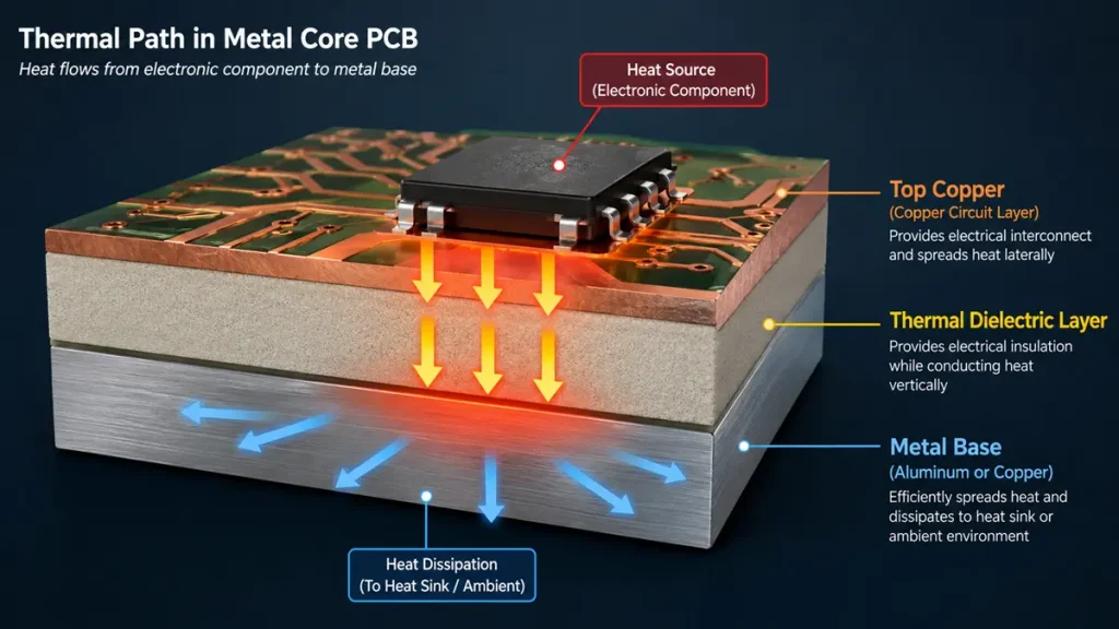
Thermal Path and Layer Structure in Metal Core PCB
Metal core PCB material — often abbreviated as MCPCB — refers to a class of printed circuit board substrates in which a metallic layer forms the structural foundation of the board rather than the conventional FR-4 glass-epoxy core. The canonical three-layer stack consists of:
- A metal base (aluminum alloy or copper alloy) that provides mechanical support and acts as the primary heat spreader
- A thermally conductive dielectric layer that electrically isolates the copper circuit from the metal base while minimising thermal resistance
- A copper circuit layer etched to the desired topology, carrying signal and power traces
The defining characteristic of any metal core PCB material is its bulk thermal conductivity — measured in W/(m·K) — which governs how quickly heat generated at the component level propagates through the board to an external heat sink or chassis. Standard FR-4 measures roughly 0.3 W/(m·K); commercial MCPCB dielectric composites currently range from 1 W/(m·K) to 8 W/(m·K), and next-generation ceramic-filled polymers entering production lines in 2026 push that figure past 12 W/(m·K).
Why Thermal Conductivity Governs Metal Core PCB Material Selection
Engineers selecting metal core PCB material are ultimately optimizing a thermal resistance budget. Every degree Celsius of junction temperature above rated limits accelerates semiconductor degradation, reduces lumen output in LED assemblies, and increases the probability of solder joint fatigue. A substrate with higher thermal conductivity reduces the temperature rise per watt of dissipated power, which either extends component life at a given power level or enables higher power in the same footprint.
However, thermal conductivity is never the only criterion. The metal base material — aluminum or copper — introduces its own trade-offs in weight, cost, coefficient of thermal expansion (CTE), and machinability. These factors, combined with MCPCB dielectric layer thickness choices, define the full design space explored in the sections below.
Aluminum Base PCB: Characteristics, Grades, and Application Fit
What Is Aluminum Base PCB and How It Differs from Standard FR-4
An aluminum base PCB substitutes an aluminum alloy plate — typically 1050, 5052, or 6061 series — for the conventional glass-epoxy core. The alloy choice affects thermal conductivity, hardness, and anodizing behavior. Series 1050 aluminum (99.5% purity) delivers approximately 229 W/(m·K) bulk conductivity and is the most common choice for general-purpose MCPCB. Series 6061, though slightly lower in conductivity (~167 W/(m·K)), offers superior mechanical strength and machinability, making it preferred in structural applications.
The bonded dielectric layer reduces the effective system-level thermal conductivity to between 1 W/(m·K) and 8 W/(m·K) depending on formulation. Despite this reduction, an aluminum base PCB transfers heat far more effectively than FR-4 — often by a factor of 10 to 20 times — making it the default choice across a wide range of thermal management applications.
Aluminum Base PCB Material Types and Thermal Conductivity Range
Commercial aluminum base PCB material suppliers — including Bergquist, Ventec, and Shengyi — offer multiple grades differentiated primarily by dielectric formulation:
- Standard grade (1.0–2.0 W/(m·K)): Epoxy-filled dielectric, cost-optimized for LED lighting drivers, consumer electronics, and SMPS units where heat loads are moderate.
- High thermal grade (2.0–4.0 W/(m·K)): Alumina or boron nitride-filled dielectric, suitable for automotive LED headlamps, industrial motor drives, and solid-state relay arrays.
- Ultra-high thermal grade (4.0–8.0 W/(m·K)): Advanced ceramic composite dielectric entering volume production in 2025–2026, targeting EV power electronics and high-flux UV LED sterilization modules.
Advantages of Aluminum Base PCB in Cost and Manufacturability
Aluminum base PCB holds a decisive cost advantage over copper core alternatives. Raw aluminum costs roughly one-fifth of an equivalent copper sheet by weight. Combined with aluminum’s lower density (2.7 g/cm³ versus 8.96 g/cm³ for copper), an aluminum base PCB is dramatically lighter — a critical factor in automotive, aerospace, and portable lighting applications where every gram is scrutinized.
From a manufacturing standpoint, aluminum machines cleanly on standard CNC routing equipment without the tool wear concerns associated with copper. Punching, shearing, and v-scoring are all routine. Anodizing provides a durable, corrosion-resistant surface finish at low cost. These manufacturability attributes allow Shenzhen Hongda Circuit Technology Co., Ltd. to offer aluminum base PCB production with competitive lead times and cost structures suitable for both prototyping and high-volume runs.
Copper Core PCB Thermal Conductivity: Performance at the Top End
What Is Copper Core PCB and Where It Is Used
A copper core PCB replaces the aluminum base with an oxygen-free high-conductivity (OFHC) copper plate, typically 0.5 mm to 3.0 mm thick. Pure copper bulk thermal conductivity measures approximately 385 W/(m·K) — 68% higher than 1050-series aluminum and more than double the conductivity of 6061 alloy. For applications where every fraction of a degree of junction temperature matters, the copper core PCB delivers thermal performance that no aluminum variant can match.
Typical application categories for copper core PCB include high-power RF amplifiers, IGBT gate driver boards, concentrated CPV (concentrating photovoltaic) receiver assemblies, precision laser diode mounts, and military-grade power conditioning modules. In each case, the higher thermal conductivity of the metal base reduces the junction-to-case thermal resistance to levels achievable in no other PCB format.
Copper Core PCB Thermal Conductivity Characteristics
The thermal conductivity advantage of copper core PCB is best understood at the system level. While the dielectric layer introduces a fixed resistance independent of the base material, the base layer itself contributes meaningfully to lateral spreading resistance — particularly for multi-chip assemblies where heat must travel horizontally across the substrate before reaching a mounting flange or cold plate. Copper’s superior lateral conductivity reduces hot-spot temperatures in multi-device layouts by 15–30% compared to an equivalent aluminum base PCB, according to thermal simulation data published in IPC technical papers through 2025.
Copper core PCB also exhibits significantly lower CTE (17 ppm/°C) compared to aluminum (23 ppm/°C), and its CTE is closer to that of ceramic capacitors, silicon devices, and GaN die. In applications subject to wide thermal cycling — such as automotive under-hood modules or outdoor base station power amplifiers — this CTE compatibility reduces solder joint fatigue and improves long-term reliability.
2026 Advances in Copper Core PCB Manufacturing Technology
PCB manufacturing technology in 2026 has introduced several refinements to copper core PCB processing. Direct copper bonding (DCB) techniques borrowed from power module substrates are being adapted to multi-layer copper core constructions, enabling two-signal-layer designs on a copper base without the registration accuracy penalties previously associated with thick-base lamination. Laser-drilled microvias down to 75 µm diameter are now compatible with copper core PCB, broadening the technology’s applicability to fine-pitch BGA packaging. Shenzhen Hongda Circuit Technology Co., Ltd. has invested in precision CNC equipment capable of holding ±0.05 mm routing tolerances on copper core PCB panels up to 600 × 500 mm, accommodating the most demanding thermal management designs entering the market.
Aluminum Base PCB vs Copper Core PCB: Direct Comparison
Thermal Conductivity Comparison
The bulk thermal conductivity of the metal base layer is the headline figure in aluminum base PCB vs copper core PCB comparisons. However, the practical delta at the system level depends heavily on the dielectric layer selection and MCPCB dielectric layer thickness. When a 3 W/(m·K) dielectric at 75 µm thickness is used on both substrates, simulations show that the junction-to-board thermal resistance differs by approximately 8–12% between aluminum and copper base — meaningful in extreme applications, but often secondary to other cost and weight factors in mainstream designs.
The gap widens significantly in three situations: (1) very high power density exceeding 50 W/cm², (2) lateral spreading over distances greater than 30 mm, and (3) applications cycling rapidly between -40 °C and +125 °C where CTE mismatch accumulates fatigue damage. In these scenarios, copper core PCB’s thermal advantages become unambiguous.
Cost, Weight, and Mechanical Properties
On a per-board basis, copper core PCB typically costs 3 to 6 times more than equivalent aluminum base PCB, depending on base thickness and panel utilization. The weight differential compounds the cost argument: a 1.6 mm copper base board weighs roughly 3.3 times as much per unit area as an equivalent aluminum base board. For most commercial LED, industrial power supply, and consumer electronics applications, these differences argue strongly in favor of aluminum base PCB.
Copper’s superior ductility is an asset in applications where the board must be formed or bent — copper core PCB tolerates mild bending without cracking, while aluminum base PCB with hard alloys may crack at sharp bend radii. Conversely, aluminum’s corrosion resistance in humid or chemically aggressive environments, when anodized, exceeds that of bare copper without surface protection.
Processing Complexity
Copper core PCB introduces machining challenges absent from aluminum base PCB work. Copper work-hardens during routing, increasing tool wear and requiring reduced feed rates. Punching thick copper base without cracking requires precisely maintained tooling clearances. Copper’s tendency to smear during drilling necessitates careful drill speed and feed optimization to achieve clean hole walls. PCB manufacturing technology advances in 2026 have improved copper core PCB machinability through the use of coated carbide tooling and high-pressure coolant delivery, but the processing remains more demanding and costly than aluminum base PCB work.
MCPCB Dielectric Layer Thickness: The Overlooked Performance Variable
Definition and Function of the MCPCB Dielectric Layer
The MCPCB dielectric layer — also called the thermal interface film or bonding prepreg — performs two physically competing functions simultaneously: it must electrically isolate the copper circuit from the metal base (typically to withstand 1,500 to 3,000 V AC in hipot testing) while conducting heat as efficiently as possible from circuit traces to the metal base. These two requirements are in direct tension: thicker dielectric provides higher electrical isolation but increases thermal resistance; thinner dielectric reduces thermal resistance but may compromise isolation voltage capability or introduce manufacturing yield risks from pinholes.
Standard MCPCB Dielectric Layer Thickness Ranges in 2026
Standard MCPCB dielectric layer thickness in current production runs from approximately 50 µm (0.05 mm) to 250 µm (0.25 mm). The table below summarizes the practical ranges and their typical application domains:
- 50–75 µm: Ultra-thin dielectric for maximum thermal performance. Used in high-flux LED lighting and EV power electronics. Requires premium dielectric materials and precise lamination control to achieve pinhole-free coverage. Withstand voltage typically 1,000–1,500 V AC.
- 75–120 µm: The most common production range. Balances thermal performance, electrical isolation, and manufacturability. Standard for LED streetlights, industrial drives, and SMPS units. Withstand voltage typically 1,500–2,500 V AC.
- 120–250 µm: Thicker dielectric for elevated isolation requirements. Used in medical equipment, high-voltage industrial applications, and designs where regulatory standards demand reinforced insulation. Thermal performance is reduced, but consistent electrical safety margins are achieved.
Relationship Between MCPCB Dielectric Layer Thickness and Thermal Resistance
Thermal resistance through the dielectric layer (R_th) follows a direct linear relationship with thickness (d) and an inverse relationship with thermal conductivity (k) and area (A): R_th = d / (k × A). Halving the dielectric thickness halves the thermal resistance through that layer. For a 100 cm² board with a 2 W/(m·K) dielectric at 100 µm thickness, the calculated dielectric thermal resistance is 0.05 °C/W — modest in isolation, but significant when device power dissipation is measured in tens of watts.
In 2025 and 2026, dielectric suppliers have introduced nano-particle filled formulations that achieve 6–8 W/(m·K) conductivity at standard 100 µm thickness, effectively delivering the thermal resistance previously only achievable at 25–30 µm with conventional materials. This allows designs to maintain established isolation voltage margins while dramatically improving thermal performance — a genuinely meaningful advance in PCB manufacturing technology.
How Dielectric Layer Thickness Affects Overall MCPCB Performance
The MCPCB dielectric layer thickness interacts with every other design variable. Thinner dielectrics magnify the importance of surface flatness on both the copper circuit layer and the metal base, since any micro-voids or air inclusions in the bond line create localized hot spots. Thinner dielectrics also reduce creepage and clearance distances, which can trigger IPC-2221 compliance issues in designs with high-voltage traces near the board edge. Engineers at Shenzhen Hongda Circuit Technology Co., Ltd. review dielectric thickness selection in the context of the complete design — circuit topology, voltage levels, expected power dissipation map, and end-use regulatory environment — rather than optimizing thickness in isolation.
How to Choose the Right Metal Core PCB Material for Your Application
Key Selection Factors: Thermal Conductivity, Cost, and Application Context
A structured selection process for metal core PCB material begins with three characterization steps. First, estimate the worst-case power dissipation map across the board, identifying peak W/cm² values and the spatial distribution of heat sources. Second, establish the maximum allowable component junction temperature based on reliability targets and regulatory constraints. Third, derive the maximum permissible junction-to-ambient thermal resistance using the system’s thermal budget. These three data points define the thermal performance requirement that the metal core PCB material must satisfy.
Once the thermal requirement is quantified, cost and manufacturability factors determine which material achieves that requirement most efficiently. In the majority of cases — LED luminaires, consumer power adapters, industrial controls, EV on-board chargers — a well-specified aluminum base PCB with an appropriate dielectric grade will satisfy the thermal budget at optimal cost. Copper core PCB is warranted when the thermal budget cannot be met in aluminum, or when CTE compatibility or lateral spreading requirements mandate it.
When to Choose Aluminum Base PCB
Choose aluminum base PCB when: power density is below approximately 30–40 W/cm², weight and cost efficiency are primary drivers, the application volume justifies standard laminate grades, regulatory isolation voltage requirements fall within the 1,500–2,500 V AC range achievable with standard dielectric formulations, and the operating temperature range does not impose extreme CTE fatigue demands. LED street lighting, architectural LED drivers, solar microinverters, household appliance control boards, and variable frequency drives in the 1–30 kW range are all natural fits for aluminum base PCB.
When to Choose Copper Core PCB
Choose copper core PCB when: thermal performance requirements exceed what aluminum base PCB can deliver at acceptable dielectric thickness, lateral heat spreading over extended distances (>30 mm) is critical, CTE compatibility with ceramic or silicon components must be maximized for long-term reliability under thermal cycling, or the application operates in a regime — military, aerospace, medical, precision RF — where performance margins take precedence over material cost. High-power laser submounts, IGBT driver boards in rail traction inverters, and concentrated solar receiver modules represent well-documented use cases.
2026 PCB Manufacturing Technology Advances Relevant to Metal Core PCB
Next-Generation Dielectric Materials for MCPCB
The most consequential PCB manufacturing technology development affecting metal core PCB selection in 2026 is the commercialization of nano-composite dielectric materials. By incorporating boron nitride nanoplatelets and alumina nanoparticles into polymer matrices at loading fractions previously unachievable without sacrificing processability, dielectric suppliers have pushed thermal conductivity past 8 W/(m·K) in production-qualified materials. This compresses the performance gap between standard aluminum base PCB and high-grade copper core PCB, enabling aluminum-based designs to address applications that previously required copper.
Embedded Component Integration in MCPCB
A growing trend in PCB manufacturing technology through 2026 is the embedding of passive and active components within the dielectric or copper layers of MCPCB constructions. By embedding bypass capacitors, current-sensing resistors, or even bare-die silicon directly in the PCB stack, engineers eliminate package resistance in the thermal path and reduce the parasitic inductance that limits switching frequency in power circuits. Shenzhen Hongda Circuit Technology Co., Ltd. has developed process capability for embedded passive components in aluminum base PCB up to four signal layers, supporting customers in next-generation GaN power module development.
Additive and Hybrid Copper Deposition for Fine-Pitch MCPCB
Fine-pitch circuit definition on metal core PCB has historically been limited by the mechanical tolerances of subtractive etch processes on thick copper foils. PCB manufacturing technology advances in 2026, drawing from semiconductor packaging techniques, have introduced semi-additive process (SAP) and modified semi-additive process (mSAP) capabilities on MCPCB substrates. These processes define conductor widths below 50 µm on metal-base boards, opening metal core PCB to applications in power conversion ICs with fine-pitch BGA footprints that were previously restricted to organic substrates with inferior thermal performance.
Summary of Metal Core PCB Material Selection Considerations
Key Comparison Points: Aluminum Base PCB vs Copper Core PCB
The aluminum base PCB vs copper core PCB decision reduces to a performance-cost trade-off calibrated against application-specific requirements. Aluminum base PCB delivers 10–20× better thermal performance than FR-4 at a fraction of copper’s cost and weight, satisfying the thermal management requirements of the vast majority of commercial power electronics and LED applications. Copper core PCB extends thermal performance by an additional 15–30% over the best aluminum alternatives, justified in high-density, high-reliability, or CTE-sensitive designs where that margin determines product success.
Role of MCPCB Dielectric Layer Thickness in Thermal Management
MCPCB dielectric layer thickness is a first-order design variable, not a detail to be left to laminate supplier defaults. Engineers who actively specify dielectric thickness — rather than accepting whatever a supplier stocks — routinely achieve 20–40% reductions in junction-to-case thermal resistance without changing the base metal. The 2026 generation of high-conductivity nano-composite dielectrics makes this variable even more powerful, delivering dielectric conductivities 2–4× higher than conventional formulations at the same production thickness.
Practical Engineering Guidance from Shenzhen Hongda Circuit Technology Co., Ltd.
Shenzhen Hongda Circuit Technology Co., Ltd. has manufactured metal core PCB assemblies across the full range of aluminum base PCB and copper core PCB materials since our establishment. Our engineering team works with customers at the design stage to model thermal resistance across the substrate stack, validate dielectric thickness against isolation voltage requirements, and select the most cost-effective material grade that satisfies the thermal budget. We maintain qualified supply chains for standard, high-thermal, and ultra-high-thermal aluminum base PCB dielectrics, as well as full copper core PCB capability in base thicknesses from 0.5 mm to 3.0 mm.
For design consultation, technical data sheets, or fabrication quotations, contact Shenzhen Hongda Circuit Technology Co., Ltd. through our engineering inquiry channels. Our team responds within one business day and can provide thermal resistance modeling as part of the quotation process for qualifying designs.
About Shenzhen Hongda Circuit Technology Co., Ltd.: A professional PCB manufacturer specializing in metal core PCB, aluminum base PCB, copper core PCB, and high-frequency circuit board fabrication. ISO9001 and IATF16949 certified. Serving customers in LED lighting, automotive, industrial, and consumer electronics sectors.
FAQs
How do I choose between an aluminum base PCB and a copper core PCB for high-power LED applications?
The choice depends heavily on your system’s total thermal dissipation targets and budget limitations. An aluminum base PCB offers a highly cost-effective, lightweight solution with standard thermal conductivity (typically 1.0 to 8.0 W/m·K at the board level), making it the industry go-to for commercial LED lighting and standard power supplies. However, if you are designing dense, ultra-high-power LED arrays where localized heat exceeds $30 \text{ W/cm}^2$, a copper core PCB is required. Copper delivers nearly double the bulk thermal conductivity of aluminum (~400 W/m·K vs. ~200 W/m·K), rapidly drawing heat away to protect component junctions, though at a higher material cost and weight.
At Shenzhen Hongda Circuit Technology Co., Ltd., we provide comprehensive DFM (Design for Manufacturing) reviews to help procurement teams balance performance and cost before production.
Why does MCPCB dielectric layer thickness matter during material selection and supplier evaluation?
The MCPCB dielectric layer thickness is the most critical bottleneck in thermal management. While the metal core (aluminum or copper) absorbs the bulk heat, the dielectric layer sits directly beneath the component and acts as a thermal barrier. According to Fourier’s Law, thermal resistance is directly proportional to dielectric thickness. A thinner dielectric layer (e.g., 38μm to 50μm) dramatically lowers thermal resistance, enabling faster heat transfer. However, it requires superior material purity to prevent electrical breakdown under high voltage.
When searching for a qualified manufacturer, ensure they can reliably laminate ultra-thin, ceramic-filled dielectrics without compromising high-voltage insulation boundaries.
What advanced 2026 manufacturing capabilities should a reliable metal core printed circuit board manufacturer possess?
As power densities increase, Tier-1 electronics buyers should vet suppliers for advanced 2026 manufacturing technologies that surpass legacy FR-4 and standard MCPCB limits. Look for vendors offering Direct-Bond Copper (DBC) or advanced thermocompression bonding, which eliminates organic adhesive layers entirely to drastically reduce thermal resistance. Additionally, ensure the supplier possesses laser-assisted micro-via drilling capabilities to support High-Density Interconnect (HDI) routing directly on metal-clad laminates.
Shenzhen Hongda Circuit Technology Co., Ltd. has fully integrated these 2026 processes, including eco-friendly nano-ceramic dielectric coatings, ensuring your boards meet both cutting-edge performance standards and global sustainability compliance.
How do the mechanical properties and processing complexities of copper core PCBs affect total acquisition cost and lead times?
Copper is a significantly denser and tougher metal than aluminum, which introduces specific fabrication challenges. A copper core PCB accelerates tool wear during mechanical drilling, routing, and punching, and requires precise environmental controls during wet chemistry processing to eliminate copper surface oxidation. These factors increase processing complexity and extended cycle times, which—combined with volatile global copper commodity pricing—results in a premium cost structure and slightly longer lead times compared to an aluminum base PCB.
To mitigate procurement risks, buyers should partner with a manufacturer that maintains stable raw material supply chains and utilizes automated CNC routing and punch-tool optimization to keep manufacturing overhead low.
What quality certifications and inspection protocols should I look for when sourcing a Tier-1 MCPCB supplier?
High thermal stress increases the risk of delamination between the metal base, dielectric, and copper circuit layers. When auditing suppliers via Google or RFQ, ensure they are certified to ISO 9001:2015, IATF 16949 (for automotive applications), and carry full UL 94V-0 flammability recognition. Your vendor must execute rigorous post-production testing, including automated optical inspection (AOI), thermal shock testing (cycling between extreme temperatures), dielectric breakdown voltage testing, and micro-section analysis to verify the integrity of the MCPCB dielectric layer thickness.
For verifiable quality reports, data sheets, or custom quotes on advanced metal core substrates, global procurement teams can contact Shenzhen Hongda Circuit Technology Co., Ltd. directly at sales@pcbkr.com.
About Author
David Chen https://www.linkedin.com/in/pcbcoming
David Chen boasts an extensive professional background in PCBA manufacturing, PCBA testing, and PCBA optimization, with specialized expertise in high-precision PCBA fault analysis and rigorous PCBA reliability testing. The author has worked with high-layer-count server PCB fabrication, ultra-low-loss backplane stackups, and thermo-mechanical reliability optimization for AI infrastructure projects involving 112G and 224G PAM4 architectures. Skilled in complex circuit design and cutting-edge advanced PCB manufacturing processes, he delivers solutions that elevate product durability and performance across industrial applications. His technical articles focusing on PCBA manufacturing workflows and testing methodologies are widely cited by industry peers, research institutions, and technical platforms, solidifying his reputation as a recognized technical authority in the global circuit board manufacturing sector.