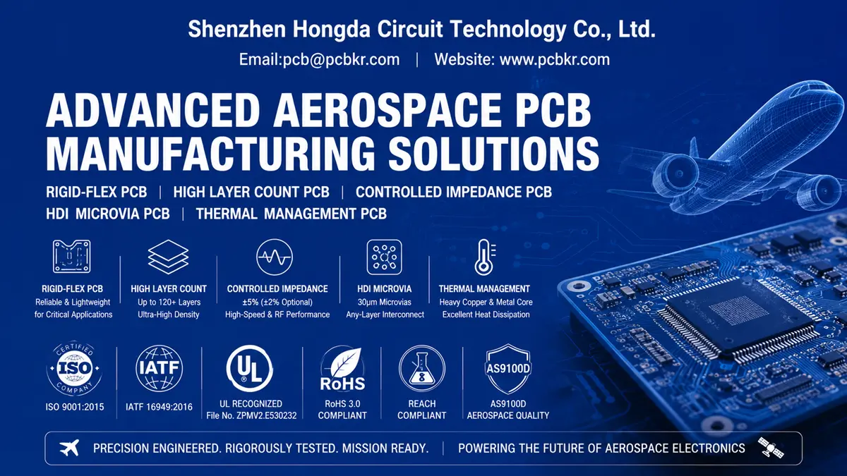
Aerospace PCB Manufacturing Capabilities (Revised & Corrected Version)
Aerospace Rigid-Flex PCB Manufacturing | Rigid Flex Aerospace Solutions for Next-Gen Avionics
What Are Aerospace Rigid-Flex PCBs and Why Do They Matter for Modern Aircraft?
Aerospace rigid-flex PCBs represent one of the most significant advancements in avionics interconnect technology, combining the structural stability of rigid boards with the mechanical flexibility of polyimide circuits in a single, monolithic assembly. In 2026, as aircraft and spacecraft systems demand ever-greater miniaturization without sacrificing reliability, rigid flex aerospace solutions have become indispensable for flight-critical applications.
At Shenzhen Hongda Circuit Technology Co., Ltd., our aerospace rigid-flex PCB manufacturing capabilities address the unique challenges of modern avionics packaging. Unlike traditional multi-board assemblies connected by cables and connectors, our rigid-flex designs eliminate up to 70% of interconnection points, dramatically reducing potential failure modes while cutting system weight by 30% and footprint by 40%. This SWaP-C (Size, Weight, Power, and Cost) optimization is critical for next-generation aircraft where every gram and cubic millimeter counts.
Typical aerospace rigid flex pcb applications include:
- Flight control system modules requiring dynamic flexing during wing deployment
- Satellite payload electronics folding into constrained launch vehicle fairings
- UAV avionics assemblies surviving high-G maneuvers and vibration
- Cockpit display interconnects routing through complex 3D geometries
Rigid Flex Aerospace Structure Types and Dynamic Bending Capabilities
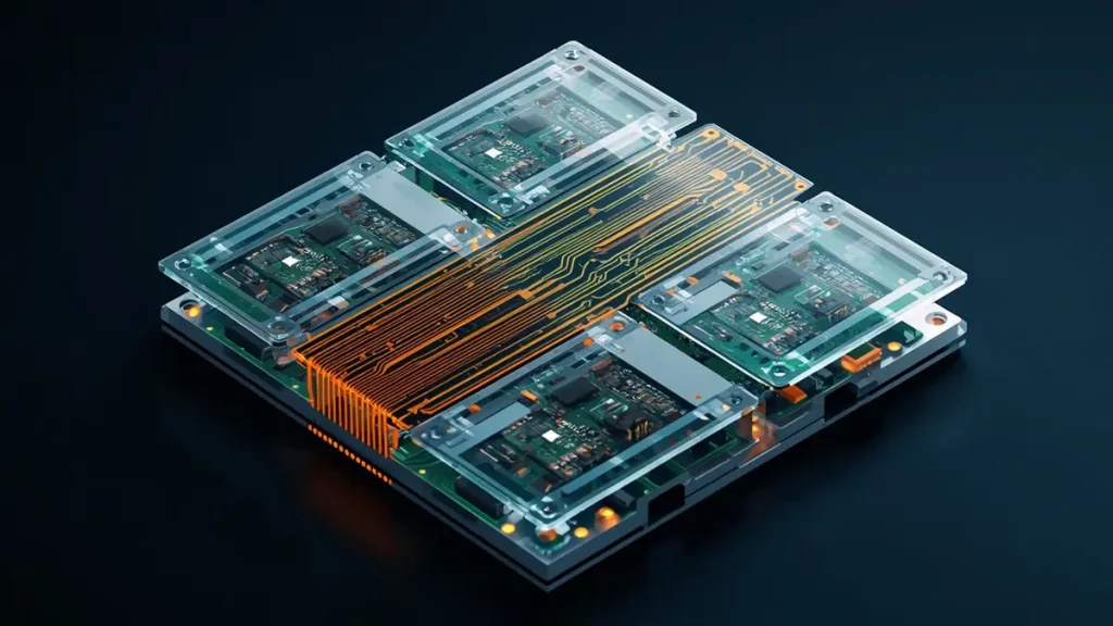
3D Technical Structure of Aerospace Rigid-Flex PCB
Our aerospace rigid-flex PCB manufacturing supports multiple structural configurations tailored to mission profiles:
Static Bend Rigid-Flex Designs: For applications where the board assumes a fixed folded position after assembly—such as satellite module interconnects—we engineer static bend zones with optimized copper grain structure and coverlay thickness. Our 2026-upgraded manufacturing lines achieve bend radii as tight as 3× the total flex thickness while maintaining IPC-6013 Class 3 reliability standards.
Dynamic Flex Rigid-Flex Designs: For systems requiring repeated flexing during operation—such as deployable antenna arrays and gimbal-mounted sensors—we implement dynamic bend zones engineered for 200,000+ flex cycles. Our proprietary stress-relief layer design and optimized transition zone coverlay tapering eliminate mechanical stress concentrations and micro-crack formation at rigid-to-flex transition zones under dynamic flexure.
Multilayer Rigid-Flex Stackups: Shenzhen Hongda Circuit Technology Co., Ltd. produces aerospace rigid-flex PCBs with up to 20 layers, integrating high-density rigid sections with ultra-thin flexible interconnects. Our 2026 process utilizes liquid crystal polymer (LCP) and PTFE flexible base materials alongside modified PI films, delivering superior high-frequency performance for 5G millimeter-wave, Satellite Ku/Ka-band, and high-speed digital signal transmission applications.
Aerospace Rigid-Flex PCB Materials and Advanced Lamination Technology
Material selection determines the ultimate reliability of rigid flex aerospace assemblies. Our 2026 material portfolio includes:
- High-Reliability Polyimide Films: Modified PI substrates with enhanced thermal stability, rated for continuous operation from -55°C to +125°C with excursion tolerance to +260°C during lead-free reflow
- LCP (Liquid Crystal Polymer) Flexible Layers: Ultra-low dielectric loss (Df < 0.002 at 10GHz) for RF and high-speed digital aerospace applications
- PTFE Composites: For extreme high-frequency requirements in satellite communication payloads
- Anti-CAF Prepreg: Cyanate ester and modified epoxy prepregs preventing conductive anodic filamentation in high-humidity aerospace environments
Our advanced lamination process employs AI-driven gradient temperature pressing with real-time pressure and temperature monitoring. The intelligent lamination system automatically adjusts parameters based on material thermal profiles, ensuring void-free bonding and precise layer registration within ±2μm—critical for maintaining impedance control across rigid-to-flex transitions.
Rigid Flex Aerospace Reliability Standards and Testing Protocols
Every aerospace rigid-flex PCB manufactured by Shenzhen Hongda Circuit Technology Co., Ltd. undergoes rigorous qualification testing:
- Thermal Cycling: 1,000 cycles from -55°C to +125°C per MIL-STD-202 Method 107
- Vibration Testing: Random vibration 20–2,000 Hz, 20G RMS per MIL-STD-810
- Mechanical Shock: 50G half-sine, 11ms duration per MIL-STD-202 Method 213
- Bend Cycle Testing: 200,000 dynamic flex cycles at specified bend radius
- Cross-Sectional Analysis: Metallographic examination of microvia plating, lamination quality, and coverlay adhesion
Our quality management system is certified to AS9100D and ISO 9001:2015, with full RoHS 3.0 and REACH compliance. All aerospace-grade rigid-flex PCBs meet or exceed IPC-6013 Class 3 performance specifications.
Aerospace Rigid-Flex PCB Process Capability Parameters
| Parameter | Mass Production Standard | Advanced Sample Capability |
|---|---|---|
| Maximum Layer Count | 20 layers (rigid) + 4 layers (flex) | 28 layers (rigid) + 6 layers (flex) |
| Minimum Line Width/Spacing | 3mil / 3mil (75μm) | 1.8mil / 1.8mil (45μm) |
| Minimum Bend Radius (Dynamic) | 5× flex thickness | 3× flex thickness |
| Minimum Bend Radius (Static) | 3× flex thickness | 2× flex thickness |
| Coverlay Material | Modified PI, LCP | PTFE composite |
| Copper Thickness (Flex) | 0.5oz – 2oz | 0.25oz – 3oz |
| Overall Thickness Tolerance | ±10% | ±5% |
| Impedance Control | ±10% | ±5% |
High Layer Count Aerospace PCB | Multilayer Avionics PCB for Complex Radar & Communication Systems
Why High Layer Count Aerospace PCBs Are Essential for Modern Avionics and Radar
As aerospace electronic systems evolve toward software-defined radios, active electronically scanned arrays (AESA), and integrated sensor fusion processors, the demand for high layer count aerospace PCBs has reached unprecedented levels. Modern radar signal processors, satellite communication payloads, and flight management computers routinely require 20+ layer stackups to accommodate dense BGA fanouts, multiple power domains, and comprehensive shielding.
Shenzhen Hongda Circuit Technology Co., Ltd. has invested significantly in ultra-high-layer manufacturing capabilities, supporting aerospace PCB layer counts from 20 layers to 120+ layers for backplane and midplane applications. Our 2026 production facility features state-of-the-art sequential lamination equipment and AI-driven registration systems that maintain layer-to-layer alignment within ±10μm—even across 30+ layer builds with total thickness exceeding 6.0mm.
The aerospace & defense PCB market was valued at approximately $3.87 billion in 2025 and is projected to reach $4.07 billion in 2026, with steady growth to $6.16 billion by 2034 at a 5.3% CAGR. This growth is driven by increasing production of next-generation aircraft, rising demand for lightweight high-density PCBs, and expansion of space electronics manufacturing.
High Layer Aerospace PCB Stackup Design and Symmetry Control
Successful high layer count aerospace PCB manufacturing begins with intelligent stackup design. Our engineering team collaborates with customers during the design phase to optimize:
Symmetric Layer Construction: For boards exceeding 16 layers, symmetric stackup design is non-negotiable to prevent warpage during thermal cycling. We employ mirrored layer sequences with balanced copper distribution, utilizing copper thieving patterns where necessary to achieve <0.75% bow and twist per IPC-6012 Class 3.
Power Integrity Optimization: High layer count aerospace designs often incorporate 8–12 distinct power rails. Our stackup planning allocates dedicated power and ground planes with optimized plane capacitance, reducing power distribution network (PDN) impedance and minimizing simultaneous switching noise (SSN) in high-speed digital systems.
Signal Layer Planning: For mixed-signal aerospace PCBs combining RF, high-speed digital, and low-noise analog circuits, we implement stripline routing with dual ground reference planes, achieving >60dB isolation between aggressive digital clocks and sensitive RF receiver front-ends.
Deep Hole Drilling and High Aspect Ratio Control for Multilayer Aerospace PCBs
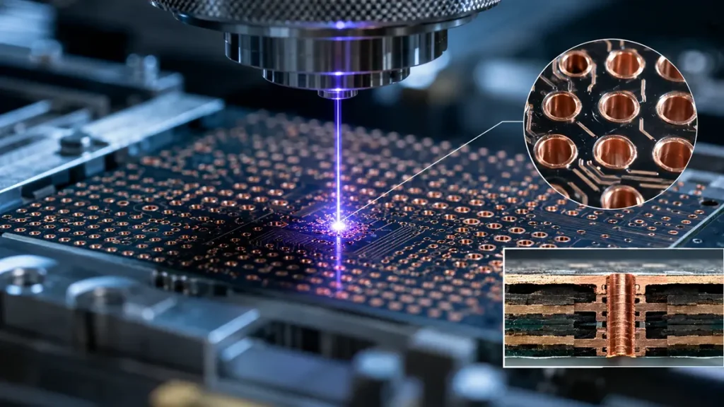
Precision UV Laser Drilling and Microvia Plating on Multilayer Aerospace PCB
High layer count aerospace PCBs present unique drilling challenges. Our 2026 manufacturing line addresses these with:
High-Aspect-Ratio Mechanical Drilling: Through-hole aspect ratios up to 20:1 (e.g. 0.30mm hole in 6.0mm thick board, or 0.50mm hole in 10.0mm thick board), utilizing precision CNC drilling with real-time breakthrough detection and automatic depth compensation. Our drilling equipment achieves positional accuracy of ±25μm with hole diameter tolerance of ±50μm.
Laser Drilling for Microvias: For buried and blind vias in high layer count builds, UV/CO₂ laser drilling systems produce microvias as small as 50μm diameter with ±5μm positional accuracy. Stacked microvia structures enable dense BGA escape routing in 0.4mm pitch and below.
Controlled Depth Drilling: Back-drilling technology removes unused via stubs in high-speed signal paths, reducing signal reflections and improving eye diagram margins in 10Gbps+ aerospace data links.
CAF Resistance and Long-Term Reliability in High Layer Count Aerospace PCBs
Conductive Anodic Filament (CAF) growth represents a critical long-term reliability concern in high layer count aerospace PCBs exposed to humid environments. Shenzhen Hongda Circuit Technology Co., Ltd. implements a multi-layer CAF mitigation strategy:
- Anti-CAF Laminate Materials: Cyanate ester and modified epoxy prepregs with enhanced resin chemistry
- Optimized Glass Styles: Reduced glass bundle diameter and improved resin wet-out to minimize conductive pathways
- Plating Process Control: Strict control of copper plating chemistry to prevent ionic contamination
- Thermal Stress Screening: 100% boards subjected to thermal stress testing per IPC-TM-650 Method 2.6.8
High Layer Aerospace PCB Manufacturing Specifications
| Parameter | Standard Capability | Advanced Capability |
|---|---|---|
| Maximum Layer Count | 28 layers | 120+ layers |
| Total Thickness | 0.4mm – 6.0mm | Up to 10.0mm |
| Minimum Hole Diameter (Mechanical) | 0.25mm (for 3.2mm board) | 0.20mm (Aspect ratio matched, up to 20:1 max) |
| Minimum Hole Diameter (Laser) | 0.05mm | 0.03mm |
| Aspect Ratio (Through-Hole) | 15:1 | 20:1 |
| Minimum Line Width/Spacing | 3mil / 3mil | 1.8mil / 1.8mil |
| Layer-to-Layer Registration | ±25μm | ±10μm |
| Bow and Twist | <1.0% | <0.5% |
Controlled Impedance PCB for Aerospace | Precision Impedance Matching for RF & High-Speed Avionics
The Critical Role of Controlled Impedance in Aerospace RF and High-Speed Systems
Aerospace electronics operate at ever-increasing frequencies. Modern radar systems transmit at X-band (8–12 GHz) and beyond, satellite communication payloads handle Ka-band (26.5–40 GHz) signals, and high-speed digital backplanes push data rates past 56 Gbps PAM4. In every case, controlled impedance PCB manufacturing is the foundation of signal integrity.
Low-Dk / Low-Df Aerospace PCB Materials for Controlled Impedance

Precision Copper Traces on High-Frequency RF Aerospace PCB
Material dielectric properties fundamentally determine achievable impedance accuracy and signal loss. Our 2026 controlled impedance aerospace PCB material portfolio includes:
M9-Grade Ultra-Low-Loss Laminates: We are among the first PCB manufacturers globally to mass-produce M9-grade substrates, officially specified by next-generation AI and high-performance computing platforms. For aerospace applications, M9 materials (Dk < 3.0, Df ≤ 0.0007 at 10GHz) deliver 30–40% lower signal loss than traditional M6/M7 generation materials, critical for long signal paths in large radar arrays and satellite payloads.
HVLP-5 Ultra-Low-Profile Copper Foil: Our HVLP5 copper foil achieves surface roughness (Rz) below 0.5μm, minimizing conductor loss at millimeter-wave frequencies. Combined with low-Dk Q-glass cloth, this material system reduces insertion loss to <0.5dB/inch at 10GHz—essential for high-frequency aerospace communication systems.
Controlled Impedance Aerospace PCB Specifications
| Parameter | Standard Tolerance | Precision Tolerance |
|---|---|---|
| Single-Ended Impedance | ±10% | ±5% (±2% available) |
| Differential Impedance | ±10% | ±5% (±2% available) |
| Maximum Operating Frequency | 40GHz | 67GHz |
| Insertion Loss (10GHz) | <1.0dB/inch | <0.5dB/inch |
| Material Dk Stability | ±3% | ±2% |
| Material Df | <0.002 | ≤0.0007 (M9 Grade) |
Microvia HDI Aerospace PCB | Aerospace HDI PCB & Microvia Technology for Miniaturized Space Electronics
Aerospace HDI PCB Structure Types: From 1+N+1 to Any-Layer Interconnect
Any-Layer Interconnect (ALI) / ELIC: The pinnacle of aerospace HDI technology, Any-Layer Interconnect enables microvia connections between any two adjacent layers throughout the stackup without a central core board. This architecture is essential for ultra-compact aerospace systems where every square millimeter of board area must be maximally utilized.
Aerospace HDI PCB and Microvia Process Capabilities
| Parameter | Mass Production | Advanced Sample |
|---|---|---|
| HDI Structure | Up to 6+N+6 | Up to 10–14 Layer Any-Layer (ELIC) |
| Microvia Diameter (Blind) | 0.05mm (50μm) | 0.03mm (30μm) |
| Microvia Diameter (Buried) | 0.15mm | 0.08mm |
| Minimum Line/Space | 1.8mil / 1.8mil | 1.0mil / 1.0mil (mSAP) |
| Maximum Layer Count | 28 layers | 78 layers |
| BGA Pitch Support | 0.4mm | 0.3mm |
| Aspect Ratio (Microvia) | 1:1 | 1.5:1 |
Thermal Management Aerospace PCB | High-Power PCB Heat Dissipation for Aerospace Electronics
Metal Core and Copper Base PCB for Aerospace Thermal Management
Embedded Copper Coin and Heavy Copper Thermal Management: Our embedded copper coin and heavy copper layer dissipation technology increases thermal dissipation efficiency by up to 300% compared to standard FR-4 structures, enabling localized heat removal from high-power integrated circuits in high-density aerospace backplanes.
Thermal Management Aerospace PCB Specifications
| Parameter | Standard Range | Extended Range |
|---|---|---|
| Copper Thickness | 2oz – 6oz | Up to 10oz+ |
| Thermal Conductivity (Dielectric) | 1.5 – 3.0 W/m·K | Up to 10 W/m·K (filled vias) |
| Metal Core / Substrate Thermal Conductivity | 200 – 400 W/m·K (Copper Base) | 170 – 230 W/m·K (AlN ceramic) |
| Maximum Operating Temperature | 130°C (standard) | 200°C+ (special materials) |
| Thermal Resistance (Junction to Board) | <0.5 K·cm²/W | <0.15 K·cm²/W (copper coin) |
| Current Carrying Capacity | Up to 50A per trace | Up to 100A+ (heavy copper) |
Shenzhen Hongda Circuit Technology Co., Ltd. — Advanced Manufacturing Infrastructure for Aerospace PCB Excellence
Quality Certifications and Aerospace Compliance
- AS9100D Aerospace Quality Management System Certification
- ISO 9001:2015 (Certificate No. 68626Q00015R000, valid through August 2029)
- IATF 16949:2016 Automotive Quality Management System
- UL Recognition (File No. ZPMV2.E530232) for multilayer and single-layer PCBs
- RoHS 3.0 and REACH full environmental compliance
- ISO 14001 Environmental Management System
Our quality system is built on IPC standards including IPC-6012 Class 3, IPC-6013 Class 3, IPC-2226, and IPC-4101E specification sheets, with full material and process traceability for every aerospace PCB we manufacture.
Frequently Asked Questions — Aerospace PCB Manufacturing
What Certifications Should I Look for in an Aerospace PCB Manufacturer?
When evaluating aerospace PCB suppliers, verify these essential certifications:
AS9100D (or transitioning to IA9100 in 2026-2027) — the aerospace-specific quality management standard adding 105+ requirements beyond ISO 9001, including product safety, counterfeit parts prevention, and configuration management
ISO 9001:2015 — foundational quality management certification
IPC-6013 Class 3 — performance specification for rigid-flex PCBs in high-reliability applications
UL Recognition — safety certification for PCB flammability and electrical performance
ITAR Registration — required for US defense-related aerospace projects
The aerospace industry is transitioning from AS9100 to IA9100 beginning in 2026, with enhanced requirements for cybersecurity, predictive quality controls, and mandatory APQP/PPAP processes. Suppliers already certified to AS9100D will have a 12–18 month advantage during this transition period.
How Do I Verify That a Supplier Can Actually Manufacture High-Reliability Aerospace PCBs?
Beyond reviewing certificates, request these verification steps:
First Article Inspection (FAI) Reports — AS9102-compliant documentation proving production capability
Process Capability Studies (Cpk) — Statistical evidence that critical parameters (impedance, plating thickness, registration) remain within specification limits
Cross-Sectional Photographs — Metallographic analysis of microvia plating, lamination quality, and copper thickness
Reliability Test Data — Thermal cycling, vibration, and mechanical shock test results
Customer References — Contact information for existing aerospace customers
Factory Audit — On-site assessment of equipment, processes, and quality systems
Be cautious of “paper certifications” — companies that pass audits without genuinely implementing quality management principles. Verify certification authenticity directly with the issuing body.
How Much Does Aerospace PCB Manufacturing Cost Compared to Standard Commercial PCBs?
Aerospace PCBs typically cost 2–5× more than equivalent commercial-grade boards due to:
Premium Materials: Aerospace-grade laminates, high-reliability copper foils, and specialized prepregs
Enhanced Process Control: Tighter tolerances, additional inspection steps, and 100% electrical testing
Documentation and Traceability: Full material certification, process records, and test reports
Lower Volume: Aerospace programs often run in batches of 100–1,000 units vs. consumer electronics at 100,000+
However, total system cost often favors aerospace-grade designs when reliability is factored in. Rigid-flex aerospace PCBs, for example, achieve 50–150 FIT (Failures in Time) compared to 200–500 FIT for traditional multi-board assemblies with connectors—a 60–70% reliability improvement that translates to substantial lifecycle cost savings.
Can Chinese PCB Manufacturers Meet US and European Aerospace Standards?
Yes — leading Chinese PCB manufacturers including Shenzhen Hongda Circuit Technology Co., Ltd. have invested heavily in certifications and capabilities to serve global aerospace markets:
Certification Alignment: ISO 9001, IATF 16949, and UL certifications are internationally recognized regardless of manufacturing location
IPC Standards Compliance: IPC-6012, IPC-6013, and IPC-2226 are global standards applied uniformly
Material Traceability: Full lot traceability from raw materials through finished product, meeting AS9102 requirements
Technical Capabilities: Chinese manufacturers now lead in HDI, rigid-flex, and high-frequency PCB technology, with many achieving capabilities matching or exceeding Western suppliers
The key is selecting a manufacturer with verified certifications, transparent quality systems, and a track record of aerospace deliveries — not assuming all suppliers meet the same standards. Request documentation, conduct audits, and validate capabilities before committing to production.
Ready to discuss your aerospace PCB requirements? Contact Shenzhen Hongda Circuit Technology Co., Ltd. today for a technical consultation, DFM review, and competitive quotation. Our engineering team specializes in translating complex aerospace designs into reliable, manufacturable, and cost-optimized PCB solutions.
Email: sales@pcbkr.com
Website: www.pcbkr.com
About Author
David Chen https://www.linkedin.com/in/pcbcoming
David Chen boasts an extensive professional background in PCBA manufacturing, PCBA testing, and PCBA optimization, with specialized expertise in high-precision PCBA fault analysis and rigorous PCBA reliability testing. The author has worked with high-layer-count server PCB fabrication, ultra-low-loss backplane stackups, and thermo-mechanical reliability optimization for AI infrastructure projects involving 112G and 224G PAM4 architectures. Skilled in complex circuit design and cutting-edge advanced PCB manufacturing processes, he delivers solutions that elevate product durability and performance across industrial applications. His technical articles focusing on PCBA manufacturing workflows and testing methodologies are widely cited by industry peers, research institutions, and technical platforms, solidifying his reputation as a recognized technical authority in the global circuit board manufacturing sector.
, and schematics detailing heavy copper PCB cross-sections, LDI, VCP plating, and laser ablation processes.](https://www.pcbkr.com/wp-content/uploads/2026/07/copper-base-pcb-quote-procurement-guide-hongda-circuit-768x429.webp)