How to Design PCBs for Ultra-Compact Wearable IoTDevices (ESP32-S3 + 4G LTE + GNSS)
Learn how to design HDI PCBs for compact wearable IoT devices using ESP32-S3, 4G LTE, and GNSS. Includes DFM guidelines, RF layout tips, and manufacturing insights from Shenzhen Hongda Circuit Technology Co., Ltd.
1. Introduction: The Technical Realities of Wearable PCB Design
The global wearable technology ecosystem is undergoing an aggressive architectural evolution. Modern market demands require electronic hardware to continuously shrink in volumetric footprint while exponentially scaling functional computing density. Contemporary wearable designs must successfully consolidate microcontrollers, cellular connectivity transceivers, global positioning chipsets, biological sensing matrices, dynamic power management units, and inductive wireless charging hardware within strict structural enclosures. This systemic compression presents hardware engineers with profound mechanical and electrical constraints, particularly when developing spatial form factors bounded within a rigid 30mm diameter envelope.
At this extreme spatial threshold, conventional multi-layer planar PCB board architectures fail completely. The physical congestion of modern product architectures—exemplified by products like the BodyLink medical fitness tracker, cellular smartwatches, and industrial lone-worker safety equipment—creates severe design bottlenecks. Engineers must resolve tight spatial boundaries, cope with multi-band radio frequency coexistence between colocated cellular and satellite
networks, and implement strategic thermal dissipation pathways under zero-airflow constraints. Achieving a fine balance between theoretical schematic excellence and high-yield volume manufacturability requires deploying advanced High Density Interconnect (HDI) manufacturing platforms, strict signal integrity verification, and comprehensive Design for Manufacturability (DFM) strategies from day one.
2. Architecture Engineering: ESP32-S3 PCB Layout and Multi-RF
Integration
System-level layout optimization for an ultra-compact architecture begins by grouping functional sub-circuits based on operational frequency, voltage sensitivity, and thermal generation profiles. The heart of modern IoT architecture features the Espressif ESP32-S3 processing core, managing primary compute tasks alongside dual-band Wi-Fi and Bluetooth Low Energy (BLE) connectivity. Surrounding this central hub is a standalone 4G LTE cellular transceiver module (such as selected solutions from Quectel or SIMCom) and an independent GNSS geolocation chipset. Each component acts as a distinct electrical node, requiring localized power configurations and isolated high-frequency return paths to maintain optimal signal performance.
Managing the multi-voltage environment requires split-plane power distribution networks capable of handling 1.8V, 3.3V, and high-current VBAT power surges. The high-speed digital buses linking the system—including Octal SPI, high-speed USB lines, and multi-channel MIPI camera or display interfaces—generate fast digital edge transitions. If unshielded, these transitions can cripple the low-noise front-ends of nearby GNSS receivers. To prevent cross-coupling, the ESP32-S3 is positioned centrally on the substrate to ensure balanced trace distribution. High-power 4G LTE modules are placed at the board edge, isolating their heavy return currents from the highly sensitive, low-amplitude GNSS receiving antennas. Every active high-frequency clock line is routed with continuous coplanar ground shielding,
preventing digital harmonics from desensitizing the integrated wireless receivers.
3. Substrate Engineering: Microvia HDI PCB Manufacturer Specifications
3.1 Recommended Stackup Configurations for Wearable Hardware
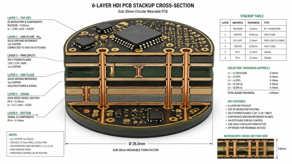
6-Layer HDI PCB Stackup Configuration for Sub-30mm Wearable IoT Devices (ESP32-S3 + 4G LTE + GNSS)
Achieving structural routing density within a sub-30mm perimeter requires moving beyond standard rigid multi-layer stacks to advanced, fine-pitch HDI architectures. Depending on design budget and electromagnetic compliance requirements, Shenzhen Hongda Circuit Technology Co., Ltd. builds these layouts on specialized 4-layer or 6-layer HDI stackups using high-Tg, low-loss halogen-free dielectric systems.
| Layer Number | Type Designation | Target Routing Functionality | Target Impedance Profiles |
|---|---|---|---|
| Layer 1 (Top) | Signal / RF Trace | Critical RF Microstrip, 0.4mm BGA Escape, Analog Front End | 50Ω RF, 90Ω USB, 100Ω Diff |
| Layer 2 | Solid Ground | Primary RF/Digital Reference Plane, Return Current Control | Continuous Reference Plane |
| Layer 3 | Power / Signal | Split Power Rails (1.8V/3.3V/VBAT), High-Speed Digital Routing | Controlled Single-Ended |
| Layer 4 | Solid Ground | Secondary Reference Plane, Shielding Layer for Bottom Elements | Continuous Reference Plane |
| Layer 5 | Power Plane | Dedicated Low-Impedance Power Routing to Peripheral Nodes | Continuous Reference Plane |
| Layer 6 (Bottom) | Signal Layer | Secondary Signal Lines, SMT Component Pads, Charging Coils | Controlled Single-Ended |
3.2 Microvia Capabilities and Advanced Interconnect Architecture
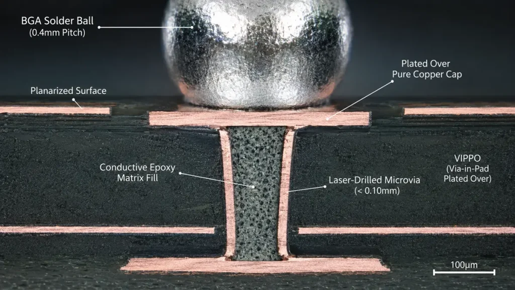
Microscopic Cross-Section of VIPPO (Via-in-Pad Plated Over) Technology with 0.4mm Pitch BGA Solder Ball
To enable reliable vertical routing transitions across these high-density layers, standard mechanical drills are replaced by specialized laser direct imaging (LDI) and UV/CO2 laser ablation systems. We manufacture microvias with laser drill diameters ≤0.10 mm, maintaining a precise capture pad diameter of ≤0.22 mm. The layer interconnect workflows support 1+N+1 and 2+N+2 staggered or stacked microvia configurations.
Crucially, implementing ultra-compact component configurations requires a reliable Via-in-Pad (VIPPO) process. Microvias hitting SMT land patterns are filled with conductive or non-conductive epoxy matrix pastes, planarized flat, and plated over with a pure copper cap. This prevents solder migration down the barrel during reflow, allowing components like 0.4mm pitch BGAs to sit directly over their vertical routing channels.
3.3 Why Mechanical and Electrical Density Matters
Moving from mechanical standard vias (minimum 0.2mm drill, 0.45mm pad) to laser-ablated microvias reclaims over 65% of local horizontal routing areas. It eliminates massive via annular rings, giving engineers the space needed to route complex 0.4mm pitch BGA breakout lines without necking down traces to unsafe manufacturing limits. Electrically, microvias minimize parasitic capacitance and inductance (L<0.5 nH), removing stub resonances to ensure clean signal transmission on high-speed digital and RF paths.
4. Geometric Precision: 0.4mm Pitch BGA Routing and Fine-Line Geometry
High-density wearable layouts require fine-line trace geometries that push conventional copper etching to its limits. Standard production lines often struggle with severe over-etching or line-width variation when handling traces under 4mils. Shenzhen Hongda Circuit Technology Co., Ltd. uses a modified Semi-Additive Process (mSAP) alongside ultrathin copper foils to reliably mass-produce uniform 3mil/3mil (0.075mm) trace width and spacing geometries.
Routing a 0.4mm pitch BGA on an ESP32-S3 or an integrated cellular baseband processor requires a precise escape strategy. Standard diagonal routing between adjacent pins is physically impossible when pin clearances drop below 0.16mm. Our recommended DFM solution uses an elite Via-in-Pad approach on the outermost pad ring. Signals drop directly from the surface landing pad down to internal Layer 2 or Layer 3 through a 0.1mm laser microvia. Inner traces then escape on these internal layers using 3mil line tracks. This layout ensures predictable impedance matching and prevents manufacturing errors like trace lifting or electrical shorts during volume production assembly.
5. Electromagnetic Harmony: RF PCB Design LTE GPS Interference Suppression
5.1 The LTE + GNSS Coexistence Challenge
Integrating multi-band 4G LTE transceivers operating between 700MHz and 2.7GHz right next to high-sensitivity GNSS receivers (GPS L1 at 1575.42MHz) creates severe electromagnetic coexistence challenges. The massive power difference is stark: an LTE power amplifier can transmit up to +33dBm, while incoming satellite tracking signals hit the antenna at a faint -130dBm to -160dBm. Without careful RF isolation, LTE transmissions can overload the GNSS low-noise amplifier (LNA), causing harmonic interference that leads to dropped satellite locks and poor tracking performance.
5.2 Layout Guidelines and Transmission Line Optimization
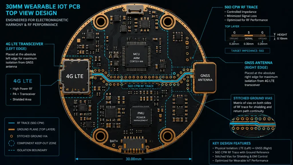
Top View Layout Design and RF Trace Optimization for Sub-30mm Wearable IoT PCB (4G LTE & GNSS Physical Isolation)
Achieving solid electromagnetic isolation requires strict physical and layout separation rules:
- Antenna Spatial Separation: Place the LTE radiator and the GNSS patch antenna on opposite sides of the 30mm PCB. Use the natural board space to maximize physical isolation, aiming for a minimum target of > 25dB out-ofband attenuation.
- 50Ω Coplanar Waveguide Control: All RF transmission lines must maintain strict 50Ω single-ended impedance. Route these paths as coplanar waveguides with a dedicated top-layer ground reference and stitched ground vias along both sides of the signal trace. This contains the electromagnetic field and prevents cross-coupling into adjacent digital lines.
- Shortest Path Routing: Keep RF paths direct, short, and free of unnecessary layer transitions. If a layer change is required, place at least two stitched ground vias right next to the signal via to maintain a continuous, low-impedance return current path.
5.3 Industrial Shielding Strategy
To block radiated noise from high-speed digital clocks and power switching components, designs must include custom surface shielding cages. We recommend a two-piece surface-mount shielding can system consisting of a low-profile frame soldered directly to the PCB during the first SMT pass, and a removable snap-on cover. This approach provides excellent Faraday cage protection while allowing easy access for debug testing, rework, or component inspection without needing to unsoldering the entire assembly.
5.4 Manufacturing Engineering and SMT Precision Control
Building high-frequency, multi-RF wearable electronics requires precise assembly tolerances. Standard SMT placement systems can allow parts to twist or shift slightly, which alters the targeted impedance matching values. We use highspeed automated placement lines equipped with sub-micron optical alignment systems to mount 01005 passives and shielding frames with exact placement accuracy. Additionally, our automated solder paste inspection (SPI) systems carefully measure paste deposition volumes down to the nanoliter, ensuring uniform solder joints and a solid, continuous electrical ground connection around the entire shielding frame perimeter.
6. Power & Thermal Management: Wearable Device PCB Assembly Optimizations
6.1 Inductive Wireless Charging Integration and Magnetic Isolation
Most modern ultra-compact wearable devices rely on wireless inductive charging (Qi or proprietary resonant protocols) to maintain a fully sealed, waterproof enclosure. Integrating the receiver coil requires reserving a clear, metal-free zone on the bottom layer of the PCB substrate. No high-speed digital traces or sensitive analog lines may cross directly over or under this charging region. Any copper plane left under the high-intensity alternating magnetic field will experience heavy eddy currents, which creates localized heat and saps power transmission efficiency. A high-permeability ferrite shielding sheet must sit between the physical coil and the PCB substrate to redirect magnetic flux away from the internal circuit layers.
6.2 Thermal Challenges in Closed Enclosures
Wearable devices operate in fully sealed polymer or bio-compatible metal housings with zero air venting. When the 4G LTE transceiver transmits data bursts, the local power amplifier generates substantial heat. Without a clear thermal escape path, local junction temperatures can quickly rise past safe limits, triggering thermal throttling in the main processor or destabilizing the clock frequency oscillators.
6.3 Structural Thermal Solutions
To manage heat in these tight spaces, the design must use the inner copper planes as a distributed heatsink. We place dense arrays of thermal microvias directly beneath the primary thermal pads of the power management IC (PMIC) and the cellular baseband chipsets. These vias connect straight to internal ground planes, letting heat spread evenly across the entire board substrate. Additionally, we recommend specifying a 2oz (70µm) copper thickness for the internal ground planes rather than standard 1oz copper. This significantly lowers thermal resistance, keeping the overall assembly operating smoothly within safe temperature margins.
7. Comprehensive DFM Checklist for Advanced Wearable PCB Projects
8. Factory Integration: Shenzhen Hongda Circuit Technology Co., Ltd. Manufacturing Capabilities
Turning high-density wearable concepts into reliable, mass-produced products requires advanced factory equipment and strict quality control. Shenzhen Hongda Circuit Technology Co., Ltd. runs an integrated, high-capacity production facility in Shenzhen, China, tailored specifically for advanced HDI fabrication and precision SMT electronics assembly.
8.1 Advanced High-Density PCB Fabrication Capabilities
- Multi-Layer HDI Processing: High-yield production lines for complex 4-to-12 layer HDI boards using advanced sequential lamination workflows.
- Precision Laser Microvias: Reliable UV/CO2 laser drilling down to ≤0.10 mm with precise alignment control for stacked or staggered microvia layouts.
- Advanced Structural Vias: In-house VIPPO (Via-in-Pad Plated Over) processes utilizing non-conductive epoxy plug fills finished with a flat copper cap.
- Strict Impedance Controls: Real-time polar impedance monitoring ensuring a tight ±10% tolerance (and down to ±5% upon request) across all high-frequency lines.
8.2 Quality Assurance and Material Integrity Verification
- High-Resolution X-Ray Inspection: Non-destructive 3D X-ray testing to check internal microvia registration, verify alignment, and ensure void-free BGA solder joints.
- Metallographic Cross-Section Analysis: Destructive physical testing on production coupons to measure plating thickness, check microvia plating quality, and verify target layer alignment.
- Automated Optical Testing: 100% AOI scanning on inner and outer layers prior to lamination, combined with highspeed flying probe testing for electrical continuity.
8.3 High-Precision SMT Micro-Assembly Capabilities
- Ultra-Fine Passive SMT Support: High-speed placement systems capable of accurately mounting next-generation 01005 and 0201 passives at volume scale.
- Fine-Pitch BGA Placement: Precision optical alignment systems that handle fine-pitch 0.4mm and 0.3mm BGA components with zero defect rates.
- Automated In-Line Inspection: Integrated 3D SPI and 3D AOI inspection systems monitoring every stage of paste deposition, part placement, and reflow profile stability.
9. Real-World Case Insight: Resolving Space and EMI Failure in a Next-Gen Medical Tracker
An international medical hardware client engaged Shenzhen Hongda Circuit Technology Co., Ltd. to salvage a failing multi-sensor wearable health tracker project. The client’s original design utilized a traditional 6-layer rigid PCB with standard mechanical vias. This layout suffered from severe structural space constraints, leaving insufficient room for a proper layout. Consequently, the close proximity of the 4G LTE antenna and the GNSS receiver caused severe electromagnetic interference, leading to frequent loss of GPS sync during cellular data bursts. Additionally, the tight, unvented enclosure trapped heat from the power components, causing the main processor to overheat and cycle reboot within minutes of operation.
Our engineering team reviewed the project files and redesigned the board onto an advanced 6-layer HDI substrate using a 1+N+1 microvia stackup. By switching to 0.1mm laser microvias and implementing a Via-in-Pad (VIPPO) configuration, we freed up over 35% of the surface routing area. This extra space allowed us to reposition the critical RF lines, establishing a clean 50Ω coplanar waveguide layout that separated the LTE and GNSS antennas to opposite sides of the board. We also integrated a low-profile, two-piece surface-mount shielding can over the digital baseband circuits and added a dense thermal via array connected to thickened 2oz internal copper ground planes.
The results were immediate. The first updated prototype run achieved stable 50Ω RF impedance control, reducing noise interference to unlock continuous, reliable GNSS satellite tracking. Thanks to the internal thermal vias and 2oz copper planes, component temperatures dropped by 14°C, completely resolving the processor overheating issue. The client approved the design after one prototyping round, moving the project smoothly into high-yield mass production at our Shenzhen factory.
10. Conclusion & Action Plan: Accelerate Your Wearable Product Launch
Designing electronics for ultra-compact wearable devices requires a careful balance between high-density routing, precise RF isolation, and smart thermal management. Every design decision-from microvia sizing to antenna spacing- directly impacts your final manufacturing yields and product stability. Working with an experienced manufacturing partner early in the design cycle is the best way to avoid costly layout mistakes and production delays.
Shenzhen Hongda Circuit Technology Co., Ltd. provides complete engineering and manufacturing support to bring your complex wearable designs to market. Send us your initial design files today, and our team will deliver a comprehensive, complimentary DFM review to optimize your stackup, check your routing tolerances, and ensure a smooth path to highyield mass production.
Optimize Your High-Density Wearable Design Today
Ready to move your project forward? Contact our engineering team at sales@pcbkr.com to receive a detailed DFM analysis and a fast manufacturing quote. Let us help you transform your complex layout into a high-performance, massproduced reality.
FAQ: Sourcing Reliable Wearable PCB Manufacturers
How do I verify if a China PCB manufacturer genuinely supports 0.4mm pitch BGA mass production for wearable devices?
True mass production of 0.4mm pitch BGAs requires an advanced factory setup. Look for suppliers that use laser direct imaging (LDI) rather than traditional film exposure, utilize modified Semi-Additive Processes (mSAP) to hold 3mil (0.075mm) lines, and have dedicated automated Via-in-Pad Plated Over (VIPPO) production lines. Always request recent factory cross-section reports and automated optical inspection (AOI) data from similar production runs to confirm their real-world capabilities.
What specific DFM parameters must an HDI PCB manufacturer provide for an ultra-compact ESP32
S3 wearable layout?
For high-density ESP32-S3 layouts, your manufacturer must specify their absolute minimum laser drill hole size (typically ≤ 0.10mm), minimum target capture pad diameter (≤ 0.22mm), and stable line/space tolerances (3mil/3mil). They must also outline their exact resin-filling and copper-cladding specs for via-in-pad structures to ensure your fine pitch components solder cleanly without assembly defects.
Why do standard multi-layer PCBs fail FCC compliance in wearable 4G LTE/GNSS designs, and how does the fabricator fix this?
Standard multi-layer boards lack the density needed for proper isolation in tight spaces. Without advanced microvias, engineers cannot route clean, continuous ground reference planes or separate sensitive RF tracks, which leads to high noise coupling and failed emissions tests. An experienced HDI fabricator resolves this by building a precise 4-layer or 6 layer microvia stackup that integrates 50Ω coplanar waveguides, embedded ground shielding shields, and dedicated surface mount frames to block unwanted radiation.
What quality control steps are required during SMT assembly to prevent solder voiding under
01005 passives and fine-pitch BGAs?
To prevent component shifts and solder voiding, the assembly facility must use 3D Automated Solder Paste Inspection (SPI) to verify exact paste volumes, run high-precision optical placement machines, and use multi-zone reflow ovens with tailored thermal profiles. Post-reflow, the factory must run 100% 3D Automated Optical Inspection (AOI) alongside high-resolution 3D X-ray testing to catch any hidden voids, shorts, or alignment issues underneath your BGA packages.
How does internal copper weight impact the thermal performance of a sealed, waterproof wearable IoT device?
Sealed wearable devices cannot use fan cooling or exterior vents, meaning all heat must dissipate through the board itself. Specifying thicker 2oz (70µm) internal copper layers instead of standard 1oz copper significantly reduces the board’s thermal resistance. This allows heat from power-heavy components like 4G LTE amplifiers to quickly spread across the entire substrate, lowering local hot spots and preventing your main processor from overheating.
About Author
David Chen https://www.linkedin.com/in/pcbcoming
David Chen boasts an extensive professional background in PCBA manufacturing, PCBA testing, and PCBA optimization, with specialized expertise in high-precision PCBA fault analysis and rigorous PCBA reliability testing. The author has worked with high-layer-count server PCB fabrication, ultra-low-loss backplane stackups, and thermo-mechanical reliability optimization for AI infrastructure projects involving 112G and 224G PAM4 architectures. Skilled in complex circuit design and cutting-edge advanced PCB manufacturing processes, he delivers solutions that elevate product durability and performance across industrial applications. His technical articles focusing on PCBA manufacturing workflows and testing methodologies are widely cited by industry peers, research institutions, and technical platforms, solidifying his reputation as a recognized technical authority in the global circuit board manufacturing sector.

, and schematics detailing heavy copper PCB cross-sections, LDI, VCP plating, and laser ablation processes.](https://www.pcbkr.com/wp-content/uploads/2026/07/copper-base-pcb-quote-procurement-guide-hongda-circuit-768x429.webp)