Why Do AI Server PCBs Generate More Heat Than Traditional Boards?
AI server PCBs generate dramatically more heat because they combine multi-kilowatt GPU power delivery, ultra-high current density, 112G/224G PAM4 signaling, and continuous tensor-processing workloads inside ultra-dense multilayer structures. Unlike traditional server boards, AI PCBs operate near simultaneous electrical, thermal, mechanical, and material reliability limits.
Why Does AI Computing Increase PCB Thermal Density Beyond Traditional Server Limits?
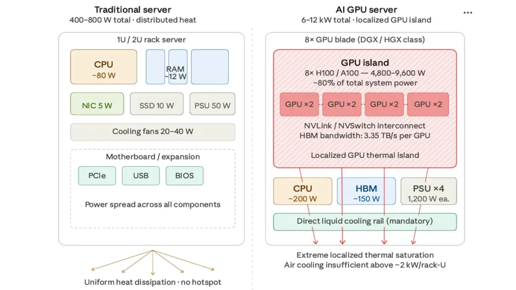
Comparison of Power Consumption Hotspots by Topology
AI clusters concentrate massive electrical power into confined accelerator regions, transforming the PCB itself into an active thermomechanical structure instead of a passive electrical carrier
Traditional enterprise motherboards distribute workloads dynamically across CPUs, memory, and storage controllers. AI platforms such as HGX, NVL72, OAM, and UBB architectures instead centralize extreme power density into localized GPU islands operating continuously at near-full utilization.
| Thermal Parameter | Traditional Server PCB | AI Server PCB (HGX/OAM/UBB) |
|---|---|---|
| Total Board Power | 400W – 800W | 6kW – 12kW |
| GPU Rail Current | 80A – 180A | 800A – 1400A |
| PCB Current Density | 15–35 A/in² | 80–200 A/in² |
| Typical Board Thickness | 1.6mm – 3.2mm | 4.5mm – 8mm |
| Localized Hotspot Temperature | 65°C – 80°C | 110°C – 135°C |
Inside modern AI systems:
- HBM stacks remain bandwidth-saturated continuously
- PCIe Gen6 and NVLink fabrics never idle
- Retimer ASICs generate persistent RF heat
- VRM power islands operate under sustained transient loading
- OAM connectors experience continuous thermal expansion cycling
Unlike conventional servers, AI workloads remove thermal recovery windows almost entirely.
This transforms PCB thermal behavior from transient heating into permanent thermal saturation.
Expert Failure Chain: AI Thermal Saturation Mechanism
Extreme GPU Current Density
→ Copper Plane Self-Heating
→ Local Resin Aging
→ Dk/Df Drift
→ Insertion Loss Increase
→ Eye Diagram Closure
→ BER Growth
→ PCIe/CXL Retraining
→ GPU Synchronization Delay
→ Cluster Efficiency Collapse
This is why AI server PCB design is rapidly evolving into a coupled thermomechanical reliability discipline rather than traditional signal routing engineering.
Why Do AI GPU Boards Produce More Heat Than Traditional CPU Motherboards?
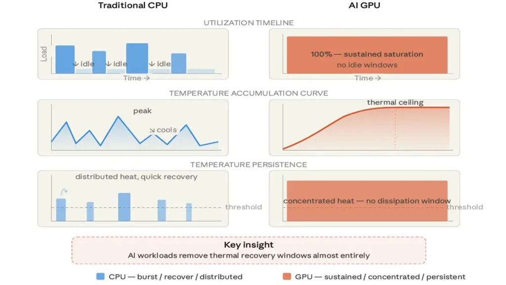
CPU vs. AI GPU: Thermal Behavior
Traditional CPUs operate with fluctuating utilization patterns, while AI accelerators maintain near-constant tensor core saturation for days or weeks.
Enterprise servers typically experience:
- 20–45% average CPU utilization
- transient power bursts
- periodic idle recovery
- moderate thermal cycling
AI training clusters instead operate at:
| Parameter | AI Cluster Operation |
|---|---|
| GPU Utilization | 95–99% |
| HBM Bandwidth Usage | Near saturation |
| Rack Power | 60kW – 120kW |
| Training Duration | 14–30 continuous days |
| Local PCB Internal Temperature | 120°C – 140°C |
The PCB underneath the GPU package becomes part of the thermal conduction path itself.
However, the true thermal danger is usually hidden internally.
Original Engineering Observation: The Real Hotspot Exists at Via-Level
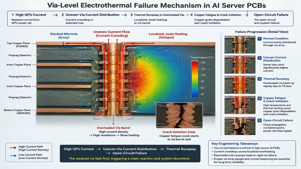
Via-Level Electrothermal Failure Mechanism in AI Server PCBs
The most dangerous thermal region inside AI PCBs is often not the GPU package surface temperature.
It is the buried microvia cluster temperature inside stacked HDI transition structures.
This distinction is extremely important.
Earlier simplified thermal models often estimate total Joule heating using:
P=I2R
For example:
- 900A GPU rail current
- 0.2mΩ localized resistance deviation
can theoretically produce:
- ~162W additional dissipation
However, this heat is NOT uniformly distributed across 1cm² copper regions.
In real AI PCB failure analysis, current crowding concentrates disproportionately into a small number of overloaded microvias or buried vias near VRM breakout regions.
The actual failure mechanism is:
- non-uniform via current sharing
- localized copper fatigue
- via barrel overcurrent
- electrothermal runaway
- rapid copper grain degradation
Instead of “uniform heating,” several overloaded microvias may individually exceed safe current density limits and fail first.
Expert Failure Chain: Via-Level Electrothermal Collapse
High GPU Current
→ Uneven Via Current Distribution
→ Current Crowding in Core Microvias
→ Localized Copper Grain Heating
→ Barrel Fatigue Acceleration
→ Intermetallic Growth
→ Via Resistance Increase
→ Additional Joule Heating
→ Thermal Runaway
→ Open-Circuit Failure
This is why AI server PCB reliability increasingly depends on via-array current balancing rather than only bulk copper thickness.
Why Do 112G and 224G PAM4 Signals Create Additional PCB Heat?
At ultra-high frequencies, PCB materials themselves convert RF electromagnetic energy directly into heat through conductor and dielectric losses.
Modern AI systems now operate with:
- PCIe Gen6
- 112G PAM4
- 224G PAM4
- CXL fabrics
- Co-packaged optics interfaces
At Nyquist frequencies above 28GHz:
- skin effect increases conductor resistance
- copper roughness amplifies scattering loss
- dielectric dissipation converts RF energy into heat
- insertion loss rises exponentially
| Nyquist Frequency | Data Rate | Typical Insertion Loss |
|---|---|---|
| 14GHz | 56G PAM4 | 0.7–1.0 dB/in |
| 28GHz | 112G PAM4 | 1.2–1.8 dB/in |
| 56GHz | 224G PAM4 | 2.5–3.8 dB/in |
Above 28GHz, even HVLP copper profile consistency becomes thermally relevant.
Manufacturing Pain Point: Backdrill Is Limited by X-Y Registration, Not Only Z-Depth
Many simplified discussions incorrectly focus only on backdrill depth tolerance.
In reality, for 24–36 layer AI backplanes:
- board thickness often exceeds 5mm
- multilayer lamination causes scale-factor distortion
- X-Y dimensional expansion becomes highly nonlinear
The true risk is:
- residual stub eccentricity
- parasitic capacitance imbalance
- differential via asymmetry
- resonant RF energy concentration
Even if Z-depth remains within ±3 mil capability, X-Y registration drift caused by lamination scaling may shift the backdrill relative to the original via centerline.
This creates:
- asymmetric residual copper stubs
- localized impedance discontinuities
- RF energy trapping zones
- additional dielectric heating
Expert Failure Chain: Backdrill Registration Failure
Thick AI PCB Lamination
→ Nonlinear Scale Expansion
→ X-Y Registration Drift
→ Stub Eccentricity
→ Parasitic Capacitance Increase
→ Local RF Reflection
→ Dielectric Heating
→ Df Drift
→ Eye Margin Collapse
→ Link Instability
This is why AI backdrill manufacturing is increasingly constrained by dimensional stability physics rather than only drilling precision.
Why Is AI PCB Cooling Now a Materials Science Problem?
Modern AI thermal performance depends heavily on laminate chemistry, filler systems, resin stability, copper profile control, and thermomechanical expansion behavior.
However, it is critical to distinguish between:
- Ultra-low-loss dielectric systems
- Thermal-enhanced low-loss dielectric systems
These are NOT identical material classes.
Material Classification Matters
Standard Ultra-Low-Loss Materials
Examples:
- Megtron 7N
- Megtron 8
- IT-988G
Typical thermal conductivity:
- ~0.35–0.45 W/m·K
Primary purpose:
- minimize dielectric loss
- improve 112G/224G insertion loss performance
Primary risks:
- brittle resin systems
- drill smear sensitivity
- low resin elasticity
Thermal-Enhanced Low-Loss Materials
These systems incorporate:
- ceramic fillers
- thermally conductive particles
- modified hydrocarbon blends
Typical thermal conductivity:
- ~0.6–1.5 W/m·K
Primary purpose:
- improve vertical heat spreading
- reduce hotspot concentration
Primary risks:
- aggressive drill-bit wear
- laser ablation instability
- filler-induced microcracking
- resin-filler interface delamination
This distinction is extremely important for accurate AI PCB thermal analysis.
Why Do OAM and UBB Connector Regions Become Hidden Thermal Fatigue Zones?
The connector interface between OAM accelerator modules and UBB baseboards experiences simultaneous electrical, thermal, and mechanical fatigue under continuous AI operation.
This is one of the least publicly discussed reliability bottlenecks in hyperscale AI systems.
In real AI racks:
- OAM modules repeatedly thermally expand and contract
- gliding connectors experience microscopic fretting motion
- high-speed differential pins experience localized RF heating
- connector solder joints accumulate cyclic mechanical strain
During long-duration LLM training:
| Parameter | Typical Range |
|---|---|
| Ambient Rack Temperature | 35°C – 42°C |
| Local Connector Hotspot | 95°C – 120°C |
| Thermal Cycling Interval | 10–15 minutes |
| Daily Thermal Cycles | 100+ |
After prolonged operation:
- contact resistance slowly rises
- insertion loss drifts upward
- localized connector heating accelerates
- retimer equalization margins shrink
- BER events begin appearing intermittently
Real Hyperscale Failure Chain: OAM Connector Fatigue
Continuous GPU Training
→ OAM Thermal Expansion
→ Connector Fretting Motion
→ Contact Resistance Increase
→ Localized Pin Heating
→ Insertion Loss Drift
→ Equalizer Margin Reduction
→ BER Instability
→ PCIe/NVLink Retraining
→ AI Cluster Performance Degradation
This is why hyperscale AI reliability engineering increasingly focuses on connector thermomechanical fatigue instead of only silicon thermals.
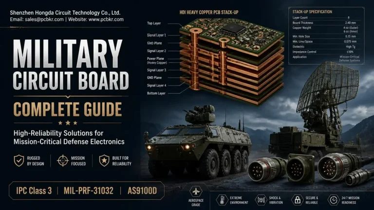
Why Are AI Server PCBs So Difficult to Manufacture Reliably?
AI PCBs simultaneously require:
- ultra-thick copper power planes
- ultra-fine HDI routing
- low-loss dielectric systems
- massive layer counts
- micron-level registration precision
- continuous high-temperature reliability
This combination pushes PCB manufacturing close to physical process limits.
| Manufacturing Parameter | AI Server PCB | Traditional Server PCB |
|---|---|---|
| Layer Count | 24–36+ | 10–18 |
| Copper Weight | 2oz–4oz | 0.5oz–1oz |
| Impedance Tolerance | ±5% | ±10% |
| Backdrill Registration | ±3 mil equivalent | ±5 mil |
| Aspect Ratio | 12:1–15:1 | 8:1–10:1 |
| Differential Pair Skew | <3ps | <10ps |
Common AI PCB yield killers include:
- resin recession
- via current imbalance
- CAF acceleration
- microvia voiding
- copper-thieving asymmetry
- scale-factor drift
- HVLP adhesion instability
- buried-via fatigue cracking
Expert Reliability Mechanism: Thermomechanical CTE Fatigue
After Tg transition:
- resin Z-axis expansion: 50–60 ppm/°C
- copper via expansion: ~17 ppm/°C
This mismatch generates severe stress concentration at:
- stacked microvia knees
- buried via interfaces
- inner-layer junctions
- HDI transition regions
Over time:
Thermal Cycling
→ Resin Expansion
→ Via Barrel Shear Stress
→ Copper Fatigue
→ Microcrack Formation
→ Resistance Instability
→ Intermittent Open Circuits
→ AI Training Failure
This is why modern AI PCB failures increasingly originate from coupled thermomechanical degradation mechanisms rather than purely electrical faults.
FAQ
Why do AI server PCBs generate more heat than traditional server boards?
Because AI accelerators continuously consume extremely high power while operating ultra-high-speed signaling fabrics and massive current-delivery networks inside dense multilayer PCB structures.
Why is via-level current crowding dangerous in AI PCBs?
Current crowding causes certain microvias to carry disproportionate current loads, accelerating localized heating, copper fatigue, and electrothermal runaway failures.
Why is backdrill X-Y registration more dangerous than simple depth tolerance?
Even if backdrill depth is correct, X-Y registration drift can create eccentric residual stubs that trap RF energy and generate localized dielectric heating.
Why must AI PCB materials distinguish between low-loss and thermal-enhanced systems?
Ultra-low-loss materials primarily optimize signal integrity, while thermal-enhanced systems additionally improve heat spreading through ceramic or conductive fillers. Their mechanical behavior and manufacturing risks differ significantly.
Why are OAM connector regions becoming a major AI reliability bottleneck?
Continuous thermal cycling and high-speed signaling create connector fretting, contact resistance growth, localized heating, and insertion-loss drift that eventually destabilize AI cluster communication links.
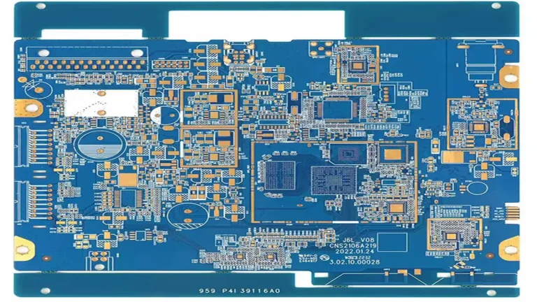
Using top-tier AI server PCB equipment to manufacture traditional PCBs delivers a strategic advantage: interlayer alignment tolerance shrinks from ±75μm to within ±25μm, and differential impedance control tightens to ±5%. Paired with 100% 3D X-Ray inspection, it grants conventional boards chip-level precision, superb signal stability, and near-100% yield.
Still, need help? Contact Us: sales@pcbkr.com
Need a PCB or PCBA quote? Quote now
About Author
David Chen https://www.linkedin.com/in/pcbcoming/
David Chen boasts an extensive professional background in PCBA manufacturing, PCBA testing, and PCBA optimization, with specialized expertise in high-precision PCBA fault analysis and rigorous PCBA reliability testing. Skilled in complex circuit design and cutting-edge advanced PCB manufacturing processes, he delivers solutions that elevate product durability and performance across industrial applications. His technical articles focusing on PCBA manufacturing workflows and testing methodologies are widely cited by industry peers, research institutions, and technical platforms, solidifying his reputation as a recognized technical authority in the global circuit board manufacturing sector.