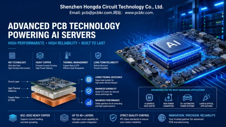
Why Is Signal Integrity More Difficult in AI Server PCBs?
Signal integrity in AI server PCBs is difficult because 112G/224G PAM4 channels are now dominated less by routing topology and more by production-induced electromagnetic variability, including dielectric phase drift, copper morphology dispersion, via resonance instability, thermal-mechanical deformation, and local manufacturing nonuniformity that conventional PCB process windows cannot statistically control.
Why Do 112G/224G PAM4 AI Channels Collapse Even When PCB Impedance Passes?
In 112G/224G PAM4 systems, static impedance compliance alone is no longer sufficient because channel stability is determined by phase consistency, resonance predictability, mode-conversion suppression, and statistical insertion-loss uniformity across production lots.
| Parameter | Simulated | Actual Production |
|---|---|---|
| SDD21 @ 26.56GHz | -18.1dB | -20.3dB |
| COM Margin | 4.7dB | 1.5dB |
| SCD21 | -43dB | -31dB |
| Return Loss | -16.4dB | -8.2dB |
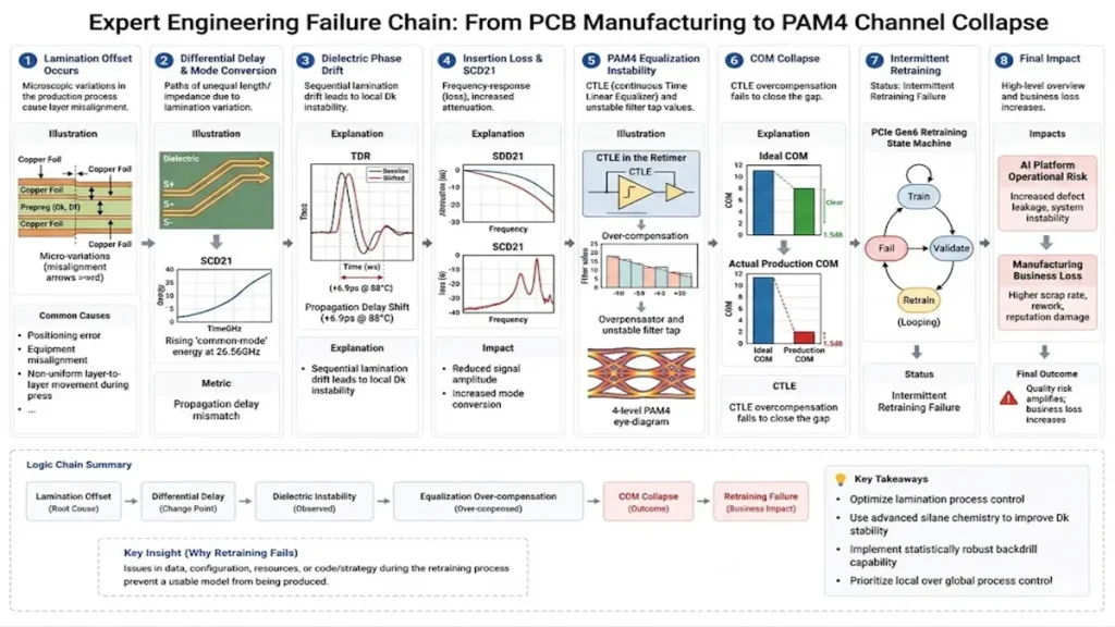
Expert Engineering Failure Chain
Sequential lamination drift → local Dk instability → propagation-delay mismatch → SCD21 degradation → CTLE overcompensation → COM collapse → retimer equalization instability → intermittent PCIe Gen6 retraining failure.
Real TDR Signature
| Metric | Measured Result |
|---|---|
| Baseline Impedance | 92Ω |
| Lowest Excursion | 84Ω |
| Highest Excursion | 109Ω |
| Ripple Periodicity | Matched 1067 Weave Pitch |
Original Manufacturing Observation
The impedance ripple did not appear in ordinary coupons because coupon structures statistically average local dielectric variation. Real AI server channels experience localized electromagnetic discontinuity caused by resin starvation and weave exposure after sequential lamination.
Why Does TCDk Drift Become More Dangerous Than Pure Insertion Loss in 112G PAM4 Systems?
In 112G PAM4 AI systems, dielectric phase instability caused by TCDk drift is often more destructive than conductor attenuation because PAM4 timing margin collapses before insertion loss reaches equalization limits.
| Mechanism | Contribution |
|---|---|
| Copper Resistivity Increase | 29% |
| Df Increase | 17% |
| TCDk-Induced Phase Drift | 54% |
Thermal Phase Drift Data
| Parameter | Room Temperature | 88°C |
|---|---|---|
| SDD21 @26GHz | -18.7dB | -20.1dB |
| Propagation Delay | Baseline | +6.9ps |
| COM Margin | 4.2dB | 1.8dB |
| BER | <1E-12 | 1E-6 |
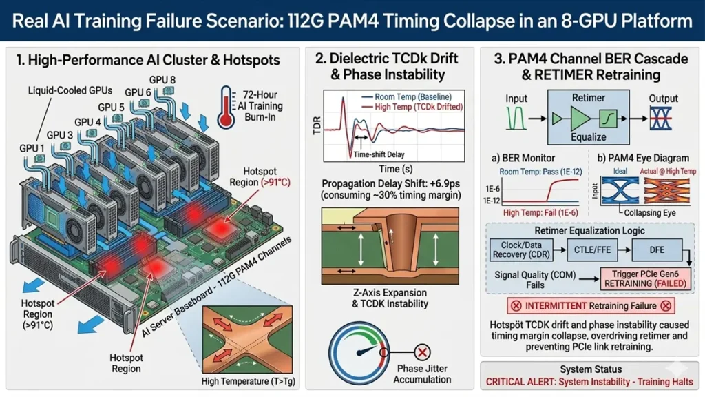
Real AI Training Failure Scenario
An 8-GPU liquid-cooled AI platform passed room-temperature validation but failed after 72-hour AI training burn-in when hotspot temperature exceeded 91°C. Local z-axis expansion and TCDk drift caused phase instability and skew accumulation, consuming nearly 30% of total PAM4 timing margin.
Why Is Copper Roughness Optimization Now a Reliability Chemistry Problem?
Reducing copper roughness improves insertion loss but simultaneously weakens resin-to-copper bonding, coupling signal integrity directly with oxide chemistry, silane treatment, CAF resistance, and thermal cycling reliability.
| Copper Type | Rz | SDD21 @28GHz |
|---|---|---|
| HVLP | 6.3μm | -1.86dB/in |
| VLP | 3.7μm | -1.43dB/in |
| ULP | 2.1μm | -1.16dB/in |
Reliability Impact
| Reliability Metric | HVLP | ULP |
|---|---|---|
| IST Cycles | 2300+ | 690 |
| CAF Resistance | Stable | Degraded |
| Peel Strength | High | Reduced |
| Rework Survivability | Stable | Weak |
Industry Correction Mechanism
Advanced AI PCB manufacturers increasingly use silane coupling agents, hybrid nano-oxide chemistry, and molecular adhesion promoters to preserve resin bonding while maintaining ultra-low-profile copper for 112G/224G insertion-loss targets.
Why Is Backdrill Capability One of the True AI Server PCB Bottlenecks?
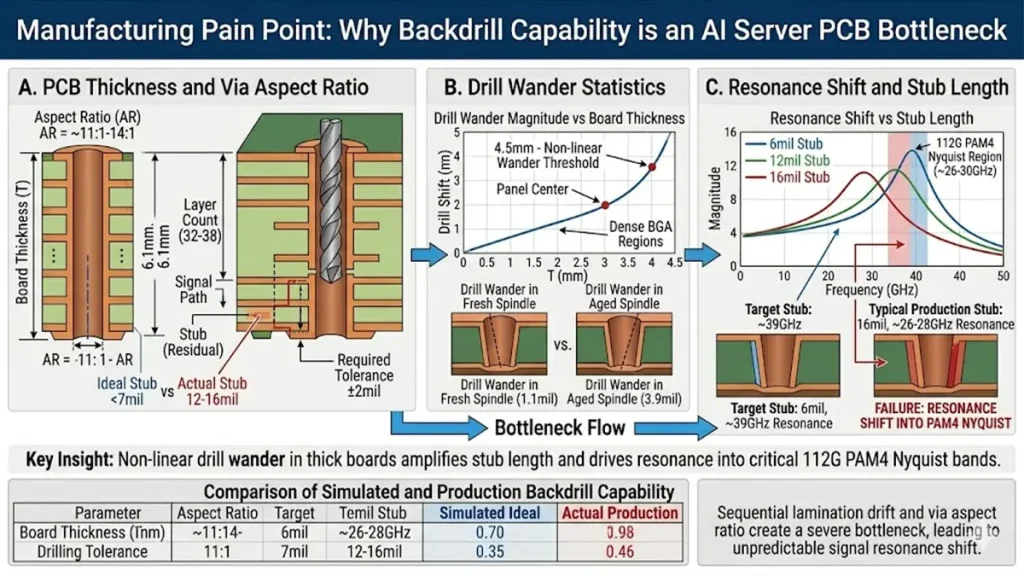
Backdrill quality is constrained by aspect ratio, spindle vibration growth, registration compensation accuracy, and residual stub predictability across thick multilayer structures.
| Parameter | Value |
|---|---|
| Board Thickness | 5.6–6.1mm |
| Layer Count | 32–38 |
| Via Aspect Ratio | 11:1–14:1 |
| Target Residual Stub | <7mil |
| Required Tolerance | ±2mil |
Drill Wander Statistics
| Condition | Drill Wander |
|---|---|
| Fresh Spindle | 1.1mil |
| Aged Spindle | 3.9mil |
Resonance Shift
| Stub Length | Resonance Frequency |
|---|---|
| 6mil | ~39GHz |
| 12mil | ~31GHz |
| 16mil | ~26–28GHz |
Manufacturing Pain Point
When board thickness exceeds 4.5mm, drill wander becomes strongly nonlinear. Residual stub distribution varies significantly between panel center and dense BGA regions, directly shifting resonance peaks into the 112G PAM4 Nyquist region.
Why Do AI Server PCB Failures Usually Originate Locally Rather Than Globally?
Most catastrophic 112G/224G failures originate from localized electromagnetic discontinuities rather than global process drift because PAM4 equalization is extremely sensitive to microscopic regional variation.
| Localized Defect | Electromagnetic Result |
|---|---|
| Resin Pocket | Phase Discontinuity |
| Weave Skew | Differential Delay |
| Desmear Recession | Impedance Depression |
| Plating Void | Return-Loss Spike |
| Oxide Nonuniformity | Localized Insertion Loss |
| Neck-Down Etch | Mode Conversion |
Real SEM Failure Analysis
During 51.2T switch qualification, cross-section SEM inspection revealed desmear over-etch reaching 18–24μm near stacked via shoulders. This created localized impedance depression below 81Ω and caused COM collapse that ordinary coupon testing failed to detect.
FAQ
Megtron 6 vs Megtron 7: Which Is Better for 112G AI Server PCBs?
Megtron 7 provides lower insertion loss, improved TCDk stability, and better phase consistency above 28GHz, making it more suitable for long AI accelerator interconnects and 224G migration.
HVLP vs ULP Copper: Which Is Better for AI Server PCB Manufacturing?
ULP copper offers lower insertion loss and higher COM margin but significantly increases reliability risk unless advanced silane-assisted oxide chemistry is implemented.
Why Can a PCB Pass Impedance Testing Yet Still Fail 112G Qualification?
Impedance coupons average behavior statistically. Real AI channels fail due to localized discontinuities including weave skew, backdrill offset, plating asymmetry, and desmear recession.
Why Is Backdrill Cp/Cpk More Important Than Layer Count?
Residual stub variability directly determines resonance stability inside the 26–30GHz region critical to 112G PAM4 signaling.
Why Do IPC-Compliant PCB Suppliers Still Fail AI Server Projects?
IPC standards mainly validate dimensional manufacturability, while AI server PCBs require statistically stable electromagnetic behavior under thermal and high-frequency operating conditions.
Using top-tier AI server PCB equipment to manufacture traditional PCBs delivers a strategic advantage: interlayer alignment tolerance shrinks from ±75μm to within ±25μm, and differential impedance control tightens to ±5%. Paired with 100% 3D X-Ray inspection, it grants conventional boards chip-level precision, superb signal stability, and near-100% yield.
Still, need help? Contact Us: sales@pcbkr.com
Need a PCB or PCBA quote? Quote now
About Author
David Chen https://www.linkedin.com/in/pcbcoming/
David Chen boasts an extensive professional background in PCBA manufacturing, PCBA testing, and PCBA optimization, with specialized expertise in high-precision PCBA fault analysis and rigorous PCBA reliability testing. Skilled in complex circuit design and cutting-edge advanced PCB manufacturing processes, he delivers solutions that elevate product durability and performance across industrial applications. His technical articles focusing on PCBA manufacturing workflows and testing methodologies are widely cited by industry peers, research institutions, and technical platforms, solidifying his reputation as a recognized technical authority in the global circuit board manufacturing sector.