Next-Gen HDI PCB Solutions by Shenzhen Hongda Circuit
Leading 2026 HDI PCB Manufacturing with mSAP and Ultra-HDI Tech
The global electronics industry in 2026 is undergoing rapid transformation driven by AI servers, 6G telecommunications, advanced wearables, and high-performance computing. As these devices continue to shrink in size while demanding faster data transmission and higher performance, HDI PCB (High-Density Interconnect Printed Circuit Board) technology has become the core foundation of modern electronic product development. HDI PCB solutions are essential to meet the strict requirements of smaller size, higher integration, and better signal integrity, making HDI PCB manufacturing a key competitive field in the global electronics supply chain.
At Shenzhen Hongda Circuit Technology Co., Ltd., we specialize in cutting-edge HDI PCB production and are at the forefront of the HDI PCB industry evolution. By integrating the most advanced 2026 manufacturing protocols, we deliver premium HDI PCB products that empower global innovators to break through technical limitations and launch next-generation electronic equipment.
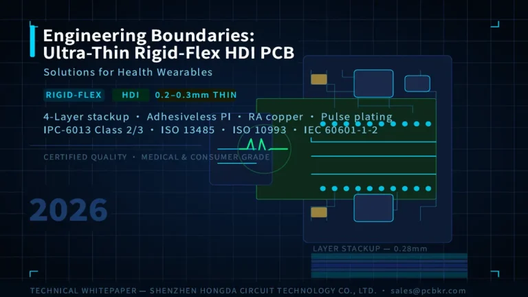
The 2026 HDI PCB Standard: Breaking Technical Barriers
Traditional standard HDI PCB manufacturing processes can no longer support the 224Gbps signal integrity required by 2026’s high-end applications. To build superior HDI PCB for next-generation hardware, we have optimized our HDI PCB production lines with three core technological pillars:
- mSAP (Modified Semi-Additive Process) for HDI PCBMoving beyond traditional subtractive etching, our mSAP technology elevates HDI PCB precision to a new level. It enables HDI PCB to achieve ultra-fine line widths and spacing (L/S) down to 15µm/15µm, which is critical for the high routing density demanded by the latest SoC and GPU architectures integrated with advanced HDI PCB.
- Sub-25µm Microvia Technology for HDI PCBOur HDI PCB adopts advanced UV-CO₂ hybrid laser drilling to realize microvia diameters below 25µm. This breakthrough allows HDI PCB to support higher layer counts and complex “Any-layer” interconnects without sacrificing board thickness or long-term reliability, making our HDI PCB ideal for compact and high-performance devices.
- Low-Loss Dielectric Integration for HDI PCBWe use 2026-grade PTFE and Thermoset materials with an ultra-low dissipation factor (Df < 0.0015) in our HDI PCB production. This material selection ensures HDI PCB delivers excellent signal transparency in high-frequency 6G and AI server applications, maintaining stable signal transmission even in complex working environments.
Advanced Cooling and Structural Integrity for HDI PCB
With rising power densities in AI-driven hardware, thermal management has become a vital part of HDI PCB design. Shenzhen Hongda Circuit embeds embedded liquid cooling channels and heavy copper layers (up to 12oz) directly into the HDI PCB stack-up. This hybrid thermal design keeps high-speed signals stable under extreme thermal loads, greatly enhancing the durability and performance of our HDI PCB.
Why Choose Shenzhen Hongda Circuit for Your HDI PCB Needs?
Developing and mass-producing high-quality HDI PCB requires professional expertise, strict quality control, and stable supply chain support. Here’s why global clients trust us for their HDI PCB projects:
- Professional HDI PCB DFM ExpertiseOur engineering team provides full Design for Manufacturing (DFM) feedback tailored for HDI PCB, helping optimize 40+ layer HDI PCB designs to shorten lead times and improve production yields, ensuring efficient HDI PCB development and delivery.
- Global Compliance for HDI PCBAll our HDI PCB products comply with the latest IPC-6012 Class 3 standards, meeting the strict certification requirements of medical, aerospace, automotive, and other high-end industries, making our HDI PCB suitable for mission-critical applications worldwide.
- Stable Supply Chain for HDI PCBWe closely monitor raw material trends and market changes to maintain a reliable supply chain for HDI PCB production. This guarantees stable pricing and on-time delivery for your HDI PCB orders, even in a volatile global market.
Conclusion
The future of electronic manufacturing is smaller, faster, and more efficient, and HDI PCB will continue to be the cornerstone of this trend. Shenzhen Hongda Circuit Technology Co., Ltd. is committed to being your long-term strategic partner, providing industry-leading HDI PCB technology, precision manufacturing, and professional services to turn your most ambitious 2026 electronic projects into reality with reliable HDI PCB solutions.
Still, need help? Contact Us: sales@pcbkr.com
Need a PCB or PCBA quote? Quote now
About Author
David Chen https://www.linkedin.com/in/pcbcoming/
David Chen boasts an extensive professional background in PCBA manufacturing, PCBA testing, and PCBA optimization, with specialized expertise in high-precision PCBA fault analysis and rigorous PCBA reliability testing. Skilled in complex circuit design and cutting-edge advanced PCB manufacturing processes, he delivers solutions that elevate product durability and performance across industrial applications. His technical articles focusing on PCBA manufacturing workflows and testing methodologies are widely cited by industry peers, research institutions, and technical platforms, solidifying his reputation as a recognized technical authority in the global circuit board manufacturing sector.