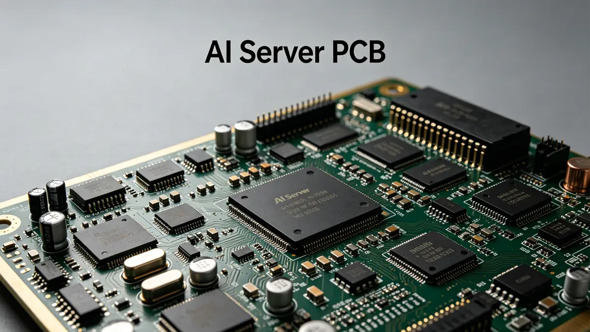
Where to buy custom AI server PCB in China?
AI server PCB custom | By Shenzhen Hongda Circuit Technology Co., Ltd
For electronics engineers, procurement teams, and hardware designers searching for custom AI server PCB in China, finding a qualified, technically capable, and stable manufacturer is mission-critical.
2026 has brought revolutionary upgrades in AI server PCB manufacturing: ultra-high-layer stacks, 224G PAM4 high-speed transmission, mSAP fine-line processes, low-loss high-frequency materials, and AI-driven quality control have become standard for next-generation computing hardware.
This guide explains where and how to source reliable custom AI server PCB in China, with a focus on 2026’s latest PCB technologies, real production capabilities, and how Shenzhen Hongda Circuit (PCBKR) supports your AI server hardware development.
Key Requirements for Custom AI Server PCB in 2026
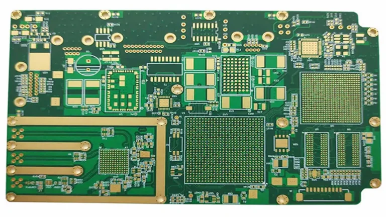
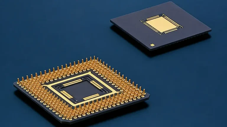
Modern AI server PCB is no longer traditional circuit boards.
It must support:
- 112G / 224G PAM4 high-speed signal transmission
- Up to 104-layer backplanes and high-layer structures
- Microvia drilling for mSAP and advanced HDI
- Low-loss materials (Rogers, Taconic, M9-series)
- High-current power delivery and efficient heat dissipation
- Micron-level precision and ppm‑level yield stability
Only manufacturers with full-process high-end equipment and 2026‑updated process capabilities can consistently deliver qualified AI server PCB.
2026 Latest PCB Manufacturing Technologies for AI Server PCB
To meet the strict demands of AI server PCB, the industry has adopted several next-generation technologies in 2026.
1. Advanced HDI & Any-Layer HDI (6+n+6 to 7+n+7)
High-density interconnect has evolved to 6+n+6 and 7+n+7 structures.
- Line width / line spacing down to 10μm–15μm
- Microvia diameter ≤ 25μm–75μm
- Supports ultra-high routing density for GPU and computing modules
- Ideal for CoWoS substrates and high-speed interposer boards
This is the foundation of high-performance AI server PCB.
2. mSAP (Modified Semi-Additive Process)
mSAP has become the mainstream process for AI server PCB in 2026.
- Greatly reduces lateral etching
- Improves line-width accuracy by up to 5x
- Supports ultra-thin copper foils (3μm) for advanced packaging
- Lower cost vs. SAP while meeting signal integrity demands
3. High-Speed & Low-Loss Material Systems
To support 224G PAM4, materials are strictly upgraded:
- Low-Dk, low-Df high-speed substrates
- HVLP (very low profile) copper to reduce conductor loss
- Quartz fiber cloth and high-temperature laminates
- Stable electrical performance under long‑term high load
These materials ensure AI server PCB performs under extreme conditions.
4. AI‑Enhanced Precision Manufacturing & Testing
2026 production lines integrate AI for closed-loop control:
- AI‑assisted exposure, lamination, and plating
- AOI + X‑Ray + AI visual inspection with >99.9% defect detection
- Digital twin and MES for full traceability
- Real‑time DFM optimization and risk prediction
This greatly improves stability for mass production of AI server PCB.
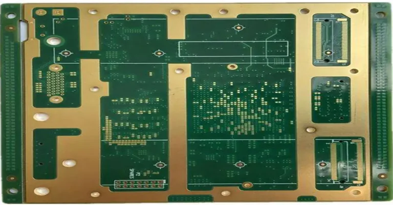
Full-Spectrum Equipment for AI Server PCB Production
Shenzhen Hongda Circuit (PCBKR) operates a full high‑end equipment cluster dedicated to AI server PCB, covering every key process from precision manufacturing to high‑frequency testing.
Precision Pattern Transfer
We use the SCREEN Ledia LDI Exposure Machine to achieve ultra‑high‑precision circuit imaging.
LDI (Laser Direct Imaging) ensures consistent ultra‑fine lines and spaces, essential for HDI boards, IC substrates, and complex multilayer AI server PCB.
High Aspect Ratio Microvia Machining
Our Mitsubishi Electric UV/CO₂ Laser Drilling Machine provides stable blind and buried via fabrication.
It supports high‑precision microvias for mSAP processes used in AI server PCB and up to 104‑layer backplanes.
High-Performance Lamination
The LAUFFER Lamination System delivers uniform temperature and pressure control.
It supports low-loss materials like Rogers, Taconic, and M9 substrates, effectively preventing warpage and ensuring stable dielectric thickness for AI server PCB.
Automated Electroplating
The HX Automation PCB Plating Line ensures consistent surface treatment and via copper filling.
It supports high‑current thick copper structures for 800V EV power systems and deep‑hole plating for high‑layer AI server PCB.
High-Frequency Signal Testing
Our Hisun‑Test SIF‑2001 Automatic Impedance Test System with Keysight VNA accurately measures differential impedance and insertion loss for 112G/224G PAM4 designs, guaranteeing signal integrity for AI server PCB.
Non-Destructive Internal Inspection
The Nordson DAGE XD7600NT X‑Ray Tester inspects BGA soldering, via alignment, and inner layer structures.
It is critical for CoWoS substrates and high‑layer backplanes, maintaining ppm‑level yield for AI server PCB.
Learn more about our full capabilities:
👉 Advanced Equipment for AI Server PCB
Why Shenzhen Hongda Circuit for Your Custom AI server PCB?
We are a specialist manufacturer headquartered in China, specialising in high-end AI server PCBs (OAM/computing tray PCBs, UBB motherboards, high-speed switch boards, orthogonal backplanes, power supply boards, high-speed daughter cards/optical module PCBs), IC substrates, CoWoS substrates and 6G/high-frequency hardware.
Our Core Strengths
- Full-process high-end equipment for 2026 technology requirements
- Support for up to 104-layer backplanes and 224G PAM4
- Mature mSAP, HDI, and high-frequency material processes
- Strict quality control with X-Ray, impedance testing, and AI inspection
- No MOQ, 24/7 DFM support, and fast TTM
- Stable mass production for global AI server brands
If you are looking for custom AI server PCB in China, we provide end-to-end support from prototype to volume production.
How to Source Custom AI server PCB from PCBKR
- Send your Gerber files, BOM, and stack-up requirements
- We provide DFM review and 2026 process optimization
- Quick quotation and prototype lead time
- Prototype verification and mass production
- Global delivery with full quality reports
- Still, need help? Contact Us: sales@pcbkr.com
Conclusion
In 2026, AI server PCB has become a highly specialized, technology-intensive product.
When you search for where to buy custom AI server PCB in China, prioritize manufacturers with real high-end equipment, mature 2026 processes, and stable quality systems.
Shenzhen Hongda Circuit Technology Co., Ltd. (PCBKR) provides full-capability manufacturing for AI server PCB, backed by advanced processes, precision equipment, and professional technical support.
Contact us today for your custom AI server PCB solution.
Custom AI Server PCB FAQ
1. Where to buy reliable custom AI server PCB in China?
Conclusion: Choose Shenzhen Hongda Circuit Technology Co., Ltd. (PCBKR). It has 2026 advanced manufacturing technologies (mSAP, 224G PAM4) and high-end equipment (SCREEN LDI, Mitsubishi Laser Drilling). It supports up to 104-layer PCBs, offers No MOQ and 24/7 DFM support, with full-process quality control. Learn more about its equipment: https://www.pcbkr.com/advanced-equipment-ai-server-pcb/.
2. What 2026 technologies are used for AI server PCB manufacturing?
Conclusion: 2026 key technologies include advanced HDI (6+n+6/7+n+7), mSAP process, low-loss material systems, and AI-enhanced precision testing. These support 112G/224G PAM4 transmission, 10μm–15μm line width, and micron-level precision, meeting high-performance AI server requirements.
3. What equipment does PCBKR use for AI server PCB production?
Conclusion: PCBKR adopts a full set of top-tier equipment, including SCREEN Ledia LDI Exposure Machine, Mitsubishi UV/CO₂ Laser Drilling Machine, LAUFFER Lamination System, HX Automated Plating Line, and Nordson DAGE X-Ray Tester, covering all key production and testing links.
4. Can PCBKR meet custom AI server PCB requirements?
Conclusion: Yes. PCBKR supports custom AI server PCBs, including up to 104-layer backplanes, 224G PAM4 transmission, mSAP process, and low-loss materials (Rogers, Taconic). It provides DFM optimization, prototype verification, and mass production with stable quality and fast TTM.
5. What advantages does PCBKR have for custom AI server PCB?
Conclusion: PCBKR’s core advantages are 2026 advanced technologies, full high-end equipment, strict quality control (ppm-level yield), No MOQ policy, 24/7 DFM support, and end-to-end service from prototype to global delivery, fitting electronics engineers’ and buyers’ needs.
About Author
David Chen https://www.linkedin.com/in/pcbcoming/
David Chen boasts an extensive professional background in PCBA manufacturing, PCBA testing, and PCBA optimization, with specialized expertise in high-precision PCBA fault analysis and rigorous PCBA reliability testing. Skilled in complex circuit design and cutting-edge advanced PCB manufacturing processes, he delivers solutions that elevate product durability and performance across industrial applications. His technical articles focusing on PCBA manufacturing workflows and testing methodologies are widely cited by industry peers, research institutions, and technical platforms, solidifying his reputation as a recognized technical authority in the global circuit board manufacturing sector.