Which PCB Materials Can Replace Standard FR-4 for PCIe 6.0?
PCIe 6.0 PCB Materials selection is critical because PCIe 6.0 operates at 64 GT/s using PAM4 signaling, which places growing emphasis on PCB dielectric loss, copper roughness, impedance consistency and overall channel design. For AI servers, accelerator cards and high-speed computing platforms, migrating from standard FR-4 to a properly selected low-loss laminate helps retain signal integrity while staying inside the allocated channel budget. That said, the most viable engineering approach is not to replace every PCB layer with pricey high-frequency material. A thoughtfully designed low-loss or hybrid stack-up delivers a better-balanced mix of electrical performance, manufacturability and material cost.
When developing PCIe 6.0 PCBs, engineers need to evaluate multiple factors holistically: dielectric performance at working frequencies, copper foil properties, transmission-line geometry, via transitions and compatibility during multilayer lamination. PCBKR provides high-speed multilayer PCB manufacturing and material evaluation services, supporting Megtron 6 and Megtron 7 hybrid stack-up schemes, controlled-impedance production, multilayer lamination and custom electrical verification to match project requirements.
Why Does PCIe 6.0 Require Better PCB Materials Than Conventional FR-4?
PCIe 6.0 doubles the data rate of PCIe 5.0 to 64 GT/s and uses PAM4 signaling to transmit two bits per symbol. This increases the importance of channel insertion loss, reflection, crosstalk, and equalization performance.
At 64 GT/s PAM4, the symbol rate is 32 GBd, corresponding to a 16 GHz Nyquist frequency. The actual channel response must be evaluated across the relevant frequency range rather than judged by a single dielectric-loss value.
Conventional FR-4 is a broad material category, not one fixed electrical specification. Different resin systems, glass styles, resin contents, and copper foil treatments can produce significantly different dielectric performance.
A conventional FR-4 construction may be suitable for some PCIe 6.0 applications when channel length and routing conditions are favorable. However, higher-loss materials can consume more of the available channel budget, leaving less margin for connectors, vias, package transitions, and other discontinuities.
Three material characteristics deserve particular attention:
- Dissipation factor (Df): Affects dielectric energy loss as signals propagate through the PCB.
- Dielectric constant (Dk): Influences propagation velocity, characteristic impedance, and signal timing.
- Copper surface roughness: Contributes to conductor loss, particularly as operating frequency increases.
Material selection should therefore be based on the complete channel design rather than a general assumption that all FR-4 materials are unsuitable for PCIe 6.0.
Which Low-Loss PCB Materials Can Replace Standard FR-4?
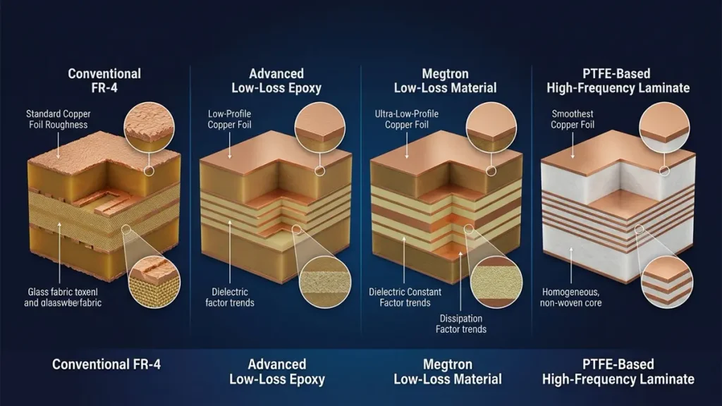
Comparison of conventional FR-4, advanced low-loss epoxy, Megtron 6, Megtron 7 and PTFE-based laminates for PCIe 6.0 high-speed multilayer PCB applications.
The most practical material replacement depends on the required channel performance, layer construction, manufacturing process, and procurement budget.
For AI computing and PCIe 6.0-related designs, engineers typically evaluate three material categories.
1. High-Speed Low-Loss Epoxy Laminates
Advanced low-loss epoxy laminates are often the first materials to evaluate when upgrading from conventional FR-4.
They offer a practical balance between electrical performance, multilayer PCB processing, and manufacturing compatibility.
Depending on the selected grade, these materials can provide improved dielectric characteristics compared with conventional FR-4 while retaining processing characteristics suitable for complex multilayer constructions.
Potential applications include:
- PCIe expansion and accelerator cards
- High-speed server motherboards
- AI computing boards
- High-speed switching and communication equipment
The exact material grade should be selected using manufacturer datasheets and electrical requirements at the relevant test frequencies.
2. Megtron Series Materials for High-Speed Multilayer PCBs
Panasonic Megtron materials are important candidates for high-speed multilayer PCB designs.
Megtron 6 and Megtron 7 can be evaluated for different electrical and stack-up requirements. The selection should consider the specific grade, dielectric construction, copper foil, and available material configurations.
For engineering teams, the benefit of the Megtron series is not simply a lower Df value. The material must also be compatible with the required layer count, impedance targets, lamination sequence, and manufacturing tolerances.
PCBKR has experience with Megtron 7 and Megtron 6 hybrid stack-up configurations. This provides a practical manufacturing basis for evaluating low-loss material combinations in high-speed multilayer projects.
A material decision should still be confirmed against the selected manufacturer’s current datasheet and the customer’s approved stack-up.
3. PTFE and Other Specialized High-Frequency Materials
PTFE-based laminates and other specialized high-frequency materials are commonly considered for applications where dielectric performance is particularly demanding.
They may be suitable for:
- RF and microwave circuits
- High-frequency communication equipment
- Specialized antenna structures
- Selected high-speed signal applications
However, PTFE-based materials should not automatically be treated as the best replacement for FR-4 in every PCIe 6.0 board.
Their processing requirements, dimensional stability, bonding compatibility, material cost, and availability must be evaluated against the complete multilayer design.
For many digital computing boards, an advanced low-loss epoxy or hybrid construction may be a more practical starting point.
FR-4 vs. Low-Loss PCB Materials: What Should Engineers Compare?
Material selection should focus on measurable electrical and manufacturing characteristics rather than generic labels such as high-speed, ultra-low-loss, or AI-grade.
| Evaluation parameter | Conventional FR-4 | Advanced low-loss materials |
|---|---|---|
| Dielectric loss | Grade-dependent | Generally lower for appropriately selected grades |
| Dielectric constant | Depends on resin and glass construction | Depends on specific material grade |
| Copper roughness | Depends on copper foil selection | Low-profile and HVLP options may be available |
| Signal integrity | Depends on channel design and material | Can provide additional channel-loss margin |
| Multilayer processing | Established manufacturing processes | Requires material-specific process qualification |
| Material cost | Generally economical | Usually higher |
| Hybrid stack-up potential | Can be combined with compatible materials | Can be selectively applied to critical layers |
The following parameters should be confirmed before approving a material substitution.
Dielectric constant (Dk)
Dk influences signal propagation velocity and transmission-line impedance. Engineers should use frequency-appropriate data rather than assuming a single Dk value applies across the entire operating range.
Dissipation factor (Df)
Df helps estimate dielectric loss. Comparisons should use consistent test frequencies and measurement methods. Values from different datasheet test conditions should not be treated as directly interchangeable.
Copper foil roughness
Copper roughness affects conductor loss and can influence high-frequency transmission performance. Low-profile or HVLP copper foil may be appropriate for critical signal layers, subject to adhesion, processing, and reliability requirements.
Dielectric thickness and stack-up geometry
The dielectric thickness between signal and reference planes affects impedance. Even when a low-loss material is selected, incorrect thickness assumptions can result in impedance deviations.
Thermal and mechanical properties
Coefficient of thermal expansion, glass transition temperature, decomposition temperature, and dimensional stability should also be reviewed for multilayer PCB reliability.
Can a Hybrid FR-4 and Megtron Stack-Up Reduce PCIe 6.0 PCB Cost?
Yes. A hybrid stack-up can be a practical solution when different PCB layers have different electrical performance requirements.
Instead of replacing every FR-4 layer with a premium low-loss laminate, engineers can selectively assign advanced materials to signal-critical portions of the PCB.
For example, a hybrid construction may use Megtron 7 or Megtron 6 in selected high-speed signal layers, while compatible FR-4 materials are retained in other portions of the stack-up.
The final arrangement depends on the electrical design and the manufacturer’s material compatibility assessment.
How to Determine Which Layers Need Low-Loss Materials
The selection process should start with the actual signal paths.
Step 1: Identify critical high-speed channels
Review PCIe differential pairs, connector transitions, package escape regions, and other critical routing paths.
Step 2: Evaluate the channel insertion-loss budget
Estimate the contribution of PCB traces, vias, connectors, packages, and other interconnect components.
Step 3: Select appropriate dielectric materials
Compare candidate laminate properties at relevant frequencies and evaluate their compatibility with the required stack-up.
Step 4: Design the hybrid construction
Determine which layers require low-loss materials and which layers can retain conventional or other compatible materials.
Step 5: Validate the complete construction
Check impedance, insertion loss, return loss, crosstalk, and other project-specific signal-integrity requirements.
A hybrid construction should never be designed by simply substituting one core material without reviewing the complete lamination structure.
Manufacturing Risks in Hybrid Multilayer Lamination
Although hybrid construction can reduce material cost, it introduces additional manufacturing considerations.
Different laminates may have different:
- Resin flow and curing characteristics
- Coefficients of thermal expansion
- Glass transition temperatures
- Thickness tolerances
- Copper adhesion characteristics
- Dimensional stability during lamination
These differences can affect layer registration, dielectric thickness, resin distribution, and final board flatness.
The lamination cycle must therefore be developed around the selected material combination.
For high-layer-count constructions, the manufacturer should review the complete press sequence, bonding requirements, material datasheets, and dimensional compensation before releasing the production stack-up.
How Does Copper Roughness Affect PCIe 6.0 Signal Integrity?
Selecting a low-loss laminate alone does not guarantee low channel loss.
Copper surface roughness also contributes to conductor loss because high-frequency current distribution is affected by the skin effect.
As frequency increases, current becomes increasingly concentrated near the conductor surface. Surface topography can increase the effective current path and contribute to additional attenuation.
For PCIe 6.0 PCB designs, engineers should consider:
- Copper foil roughness on critical signal layers
- Copper foil treatment and adhesion requirements
- Trace width and dielectric spacing
- Differential pair geometry
- Reference-plane continuity
- Via transitions and backdrilling requirements
The appropriate copper foil should be selected together with the laminate and routing geometry.
Using a lower-profile copper foil may improve high-frequency conductor performance, but its suitability must also be confirmed for adhesion, lamination, and long-term reliability.
How Does Multilayer Lamination Affect PCIe 6.0 PCB Reliability?
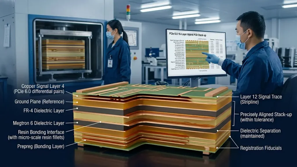
Multilayer PCB lamination process illustrating FR-4 and Megtron material compatibility, copper layer alignment, dielectric bonding and dimensional stability in high-speed PCB manufacturing.
High-speed accelerator cards and server boards frequently require complex multilayer structures.
As layer count increases, the manufacturing challenge extends beyond simply maintaining the specified dielectric thickness.
The manufacturer must control:
- Inner-layer registration
- Dielectric thickness consistency
- Resin flow and distribution
- Lamination pressure and temperature
- Interlayer bonding
- Dimensional stability after lamination
These factors directly affect impedance consistency and multilayer reliability.
In hybrid Megtron and FR-4 constructions, the lamination process requires particular attention because different material systems may respond differently to heat and pressure.
PCBKR uses LAUFFER lamination equipment with controlled pressure settings of 80, 150, and 200 psi, together with vacuum processing below 50 mbar.
The actual press recipe must be established for the selected material combination, copper distribution, board thickness, and layer structure. These equipment parameters are manufacturing capabilities, not universal lamination specifications for every Megtron stack-up.
Layer registration and dimensional compensation should also be reviewed before production to reduce the risk of misalignment and dielectric construction deviations.
How Does PCBKR Control Impedance in High-Speed Multilayer PCBs?
Controlled impedance is a manufacturing requirement that connects material selection, stack-up engineering, and final electrical performance.
Even a low-loss laminate cannot deliver the expected signal performance if the finished transmission-line geometry differs significantly from the design.
PCBKR evaluates impedance-related manufacturing parameters through the following processes.
Stack-Up and DFM Review
Before fabrication, the manufacturing team reviews the customer’s Gerber files, stack-up, dielectric thickness, copper weight, and impedance requirements.
The purpose is to identify potential manufacturing issues before production, including:
- Incompatible material combinations
- Insufficient dielectric thickness
- Trace geometry limitations
- Copper distribution differences
- Critical layer registration requirements
Controlled Impedance Fabrication
The fabrication process must maintain the specified trace width, spacing, copper thickness, and dielectric geometry.
PCBKR’s manufacturing capabilities include advanced multilayer fabrication and controlled-impedance processing.
The final impedance tolerance is defined according to the approved customer specification and the feasibility of the actual stack-up.
TDR Verification
Time-domain reflectometry (TDR) is used to evaluate characteristic impedance along controlled-impedance structures.
Impedance coupons can be included in the manufacturing panel according to the agreed test plan.
Coupon results should be interpreted in the context of the actual stack-up and routing geometry. A coupon measurement alone does not establish the insertion-loss performance of every functional signal channel.
VNA Testing
A vector network analyzer (VNA) can be used to characterize frequency-domain electrical behavior, including insertion loss and return loss, when appropriate test structures and calibration methods are available.
PCBKR has VNA testing capability up to 70 GHz. The actual test frequency, fixture, calibration, and acceptance criteria must be agreed for each project.
This capability supports high-frequency PCB evaluation, but does not independently establish PCIe 6.0 protocol compliance.
What Should Engineers Verify Before Replacing FR-4 in a PCIe 6.0 PCB?
Before approving a new material, engineering and procurement teams should complete a structured technical review.
| Verification item | Required engineering information |
|---|---|
| Target interface | PCIe generation and data rate |
| Channel requirements | Insertion-loss and return-loss budget |
| Material selection | Manufacturer and exact laminate grade |
| Dielectric properties | Dk and Df with test frequency and method |
| Copper specification | Foil type and roughness |
| Stack-up | Layer count, copper weights, dielectric thickness |
| Impedance | Single-ended or differential target and tolerance |
| Via structure | Through, blind, buried, or backdrilled vias |
| Lamination | Material compatibility and press process |
| Electrical testing | TDR, VNA, and project-specific test structures |
For procurement teams, requesting a material substitution without a revised stack-up and manufacturing review can create unnecessary engineering iterations.
A better approach is to provide the PCB manufacturer with the existing stack-up, Gerber files, impedance requirements, target channel performance, and preferred material options.
This allows the manufacturer to evaluate the replacement material based on the actual board construction rather than a generic material recommendation.
How PCBKR Supports Megtron-Based High-Speed Multilayer PCB Manufacturing
PCBKR, operated by Shenzhen Hongda Circuit Technology Co., Ltd., provides PCB fabrication and PCBA manufacturing services for industrial electronics, communication equipment, and high-speed computing applications.
For advanced multilayer PCB projects, PCBKR’s relevant manufacturing capabilities include:
Megtron material and hybrid stack-up evaluation
PCBKR has experience with Megtron 7 and Megtron 6 hybrid stack-up configurations. Material selection and layer allocation are evaluated against the customer’s electrical and manufacturing requirements.
Controlled multilayer lamination
LAUFFER lamination equipment supports controlled pressure and vacuum processing. Press parameters are determined according to the selected materials and approved construction.
Precision imaging and registration
SCREEN Ledia LDI equipment supports fine-line imaging, with an 8 μm imaging target. The applicable production tolerance depends on the complete process and design requirements.
Impedance and electrical verification
TDR-based impedance evaluation and VNA testing up to 70 GHz support electrical characterization according to the agreed project test plan.
Engineering and manufacturing coordination
PCBKR reviews Gerber data, stack-up information, material specifications, and production requirements before manufacturing. This helps identify material compatibility and process risks before production release.
The final material, stack-up, impedance tolerance, and test coverage must be confirmed for each individual project.
FAQ: PCIe 6.0 PCB Material Replacement
Can standard FR-4 be used for PCIe 6.0 PCBs?
It depends on the channel design, PCB thickness, routing length, connectors, and available signal-integrity margin. Some designs may work with selected FR-4 grades, while more demanding channels may require low-loss materials to meet insertion-loss requirements.
Which materials are suitable for replacing FR-4 in PCIe 6.0 designs?
Advanced low-loss epoxy laminates, Megtron 6, Megtron 7, and selected specialized high-frequency materials can be evaluated. The correct choice depends on the target electrical performance, material availability, and manufacturing compatibility.
Is Megtron 7 better than Megtron 6 for PCIe 6.0?
The answer depends on the exact material grade, electrical requirements, stack-up, and project cost. Engineers should compare manufacturer datasheets at consistent test conditions rather than selecting a material based only on its product series.
Can FR-4 and Megtron be combined in one multilayer PCB?
Yes, compatible materials can be combined in a hybrid stack-up. However, resin systems, thermal expansion, curing behavior, dielectric thickness, and lamination conditions must be evaluated before production.
How does PCBKR verify impedance in high-speed multilayer PCBs?
PCBKR supports controlled-impedance fabrication and TDR-based verification. VNA testing up to 70 GHz is also available for agreed electrical characterization requirements. Complete PCIe channel validation requires appropriate test structures, fixtures, calibration, and project-specific acceptance criteria.
Request a PCIe 6.0 PCB Material and Stack-Up Review
Choosing a replacement for conventional FR-4 is an engineering decision involving dielectric properties, copper roughness, impedance geometry, multilayer lamination, and electrical verification.
For AI server, accelerator card, and high-speed computing PCB projects, PCBKR can review your material requirements and evaluate suitable Megtron-based or other compatible low-loss stack-up options.
To support an engineering review, please provide:
- Gerber files or preliminary PCB layout
- Existing or proposed stack-up
- Target PCIe interface and data rate
- Impedance requirements
- Preferred laminate materials
- Board thickness and layer count
- Electrical testing requirements
Contact PCBKR for PCB Manufacturing and PCBA Assembly
Email: sales@pcbkr.com
Website: https://www.pcbkr.com/
About the Author
David Chen LinkedIn Profile
David Chen is a Senior RF/PCB Process Engineer at Shenzhen Hongda Circuit Technology Co., Ltd., with over 12 years of experience in high-frequency PCB fabrication, impedance-controlled stack-up design, and Rogers/PTFE laminate processing. He also boasts an extensive professional background in PCBA manufacturing, PCBA testing, and PCBA optimization, with specialized expertise in high-precision PCBA fault analysis and rigorous PCBA reliability testing. The author has worked with high-layer-count server PCB fabrication, ultra-low-loss backplane stackups, and thermo-mechanical reliability optimization for AI infrastructure projects involving 112G and 224G PAM4 architectures. Skilled in complex circuit design and cutting-edge advanced PCB manufacturing processes, he delivers solutions that elevate product durability and performance across industrial applications. His technical articles focusing on PCBA manufacturing workflows and testing methodologies are widely cited by industry peers and technical platforms, and have gained attention and recognition from industry colleagues.