Industrial IoT Embedded Component PCB Guide: DFM, Cavity Fabrication & Reliability Qualification
Industrial IoT embedded component PCBs integrate selected passive or active devices inside the multilayer board to increase functional density, recover surface area, shorten critical interconnects, and improve packaging efficiency. They are especially useful for compact industrial sensors, remote I/O, PLC modules, edge controllers, gateways, and condition‑monitoring equipment.
Industrial IoT equipment creates a difficult PCB design combination: small mechanical envelopes, continuous operation, electrical noise, 24 V industrial power, vibration, thermal cycling, communication interfaces, and long service life.
That changes the engineering question.
The objective is not simply to determine whether a resistor, capacitor, IC, or die can be embedded. The real question is whether the embedded structure can maintain electrical, mechanical, thermal, and manufacturing performance throughout the product life cycle.
For Shenzhen Hongda Circuit Technology Co., Ltd., we approach an Industrial IoT embedded PCB as an integrated manufacturing problem involving component geometry, cavity tolerance, layer registration, dielectric structure, microvias, lamination, copper distribution, thermal paths, inspection, and reliability validation.
Why Are Embedded Component PCBs Valuable in Industrial IoT Devices?
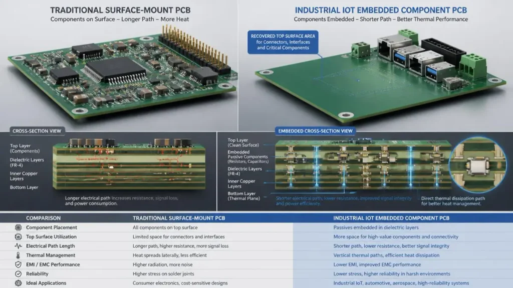
Industrial IoT Embedded Component PCB vs Traditional SMT Comparison – Hongda Circuit
Embedded components are valuable in Industrial IoT products when they solve a specific system‑level constraint such as limited enclosure volume, routing congestion, electrical parasitics, thermal density, or component‑placement restrictions. The technology is most effective when the embedding decision is made together with PCB stack‑up, signal integrity, thermal design, and DFM.
Industrial IoT products are rarely constrained by only one engineering variable.
A remote sensor may have a 60–100 mm enclosure while needing:
- MCU or processor
- Sensor front end
- Memory
- Power conversion
- ESD protection
- Communication interface
- Filtering
- Status indicators
- Connector or terminal block
A conventional surface‑mount architecture can consume a significant portion of the available top and bottom surface.
Embedding selected components moves some functions into the PCB structure.
The resulting benefit can be expressed more accurately as:
Available surface area = Original surface area − embedded component footprint
But area reduction is only one part of the equation.
For Industrial IoT designs, engineers should evaluate:
Area + electrical path length + thermal path + EMC + mechanical stress + repairability + manufacturing yield
rather than treating miniaturization as the sole objective.
IPC‑7092 specifically addresses design and assembly process implementation for embedded components, while IPC‑6012F includes active/passive embedded circuitry within its rigid printed‑board qualification and performance scope. For cross‑industry embedded‑component PCB fundamentals, general‑purpose design challenges and supplier qualification workflows, please refer to our Embedded Component PCB: Technology, Manufacturing & Procurement Guide.
Which Industrial IoT Applications Benefit Most From Embedded Components?
The strongest candidates are compact sensor nodes, remote I/O modules, PLC electronics, industrial Ethernet gateways, edge controllers, motor‑monitoring systems, smart meters, and condition‑monitoring devices where PCB area, EMC, routing density, or environmental reliability creates a measurable design constraint.
Industrial Sensor Nodes
A vibration, pressure, temperature, flow, or current‑monitoring node often combines several sensitive analog functions with digital processing and communication.
A representative architecture may contain:
Sensor → Analog Front End → ADC → MCU → Memory → Communication → Power
The PCB challenge is not simply component count.
Sensitive analog traces may need separation from:
- DC/DC switching nodes
- clock lines
- Ethernet PHY signals
- relay drivers
- motor‑control interfaces
- high‑current copper
Embedding selected passive networks can free the surface for connectors and larger components while allowing engineers to optimize critical electrical paths.
Remote I/O Modules
Remote I/O products commonly combine multiple input/output channels with isolation, protection, communication, and power conversion.
A typical industrial architecture may include:
- 24 VDC input
- reverse‑polarity protection
- transient protection
- isolated DC/DC
- digital input conditioning
- analog input filtering
- MCU
- RS‑485, CAN, or Ethernet
- isolated communication
- status monitoring
Here, embedding is particularly useful when the enclosure height and PCB area are both restricted.
Industrial Ethernet Gateways
Industrial Ethernet introduces additional layout sensitivity.
The board may contain:
- Ethernet PHY
- magnetics or integrated magnetics interface
- oscillator
- MCU/MPU
- memory
- DC/DC converters
- ESD protection
- common‑mode filtering
The embedding strategy should therefore be selective.
A component that improves density but complicates a high‑speed differential path may not be worth embedding.
Motor Condition‑Monitoring Equipment
Motor‑monitoring electronics operate close to sources of electromagnetic interference and mechanical vibration.
The PCB may simultaneously process:
- accelerometer signals
- temperature measurements
- current measurements
- rotational information
- wired communication
- wireless communication
This makes mechanical integrity and EMC just as important as electrical density.
Which Components Should Be Embedded in an Industrial IoT PCB?
Embedded resistors and capacitors are generally the easiest starting point, while inductors, packaged active devices, and semiconductor dies require progressively more demanding thermal, mechanical, interconnection, and process analysis.
Embedded Resistors
Embedded resistors are useful for:
- pull‑up/pull‑down networks
- signal termination
- bias networks
- sensor conditioning
- voltage‑divider functions
- selected filtering circuits
For a resistor structure, the engineer must consider more than resistance value.
Important variables include:
Sheet resistance + geometry + copper thickness + etch factor + tolerance + temperature coefficient + power density
For formed embedded resistors, final resistance depends on the effective geometry after fabrication.
A useful conceptual relationship is:
R ≈ Rs × L/W
where:
- R = resistance
- Rs = sheet resistance
- L = effective resistor length
- W = effective resistor width
This is why fabrication tolerances can directly affect electrical tolerance.
Embedded Capacitors
Embedded capacitors are particularly interesting for local decoupling and power‑integrity applications.
The fundamental relationship remains:
C = εA/d
where:
- C = capacitance
- ε = dielectric permittivity
- A = effective electrode area
- d = dielectric thickness
Reducing dielectric thickness increases capacitance for a given area.
However, an Industrial IoT designer should also consider:
- DC bias
- temperature coefficient
- dielectric loss
- leakage
- voltage rating
- aging
- manufacturing tolerance
The correct question is therefore not:
“Can this capacitor be embedded?”
It is:
“Does the embedded capacitor provide sufficient electrical benefit without creating an unacceptable reliability or manufacturing risk?”
Embedded Inductors
Embedded inductors can support:
- filtering
- power conversion
- RF functions
- EMI suppression
But inductors are more difficult to evaluate because magnetic coupling, core material, geometry, current density, saturation and thermal behavior may dominate the design.
Embedded Active Devices
Embedding active components can reduce package‑related volume and potentially shorten interconnections.
However, active‑device embedding requires a much more comprehensive analysis of:
Thermal resistance + warpage + interconnection + dielectric protection + inspection + reliability
For many Industrial IoT products, passive embedding is therefore the more practical starting point.
Embedded Dies
Bare‑die embedding is an advanced architecture that moves PCB manufacturing closer to electronic packaging.
It may be justified when:
- package height is highly constrained
- routing density is extreme
- electrical path length must be minimized
- system integration benefits outweigh manufacturing complexity
IPC‑7092 covers embedded active and passive circuitry, while IPC‑7094 addresses flip‑chip and die‑size component implementation.
How Should Embedded Components Be Positioned in Industrial IoT PCBs?
Component placement should be driven by electrical function, thermal behavior, mechanical constraints, cavity geometry, and downstream manufacturing access rather than by surface‑area reduction alone.
This is one of the most important differences between a conventional SMT layout review and an embedded‑component review.
Consider a compact industrial sensor.
The designer may want to place a filtering capacitor immediately below the sensor or MCU.
Electrically, that can be attractive.
Manufacturing‑wise, however, the position must also be checked against:
- cavity edge
- copper planes
- adjacent vias
- microvia landing area
- dielectric thickness
- lamination flow
- registration tolerance
A useful engineering rule is to divide the embedded area into three zones:
Zone 1 — Functional Area
The component and its immediate electrical connections.
Zone 2 — Manufacturing Clearance
The space required for cavity formation, placement and registration.
Zone 3 — Structural Area
The surrounding dielectric and copper structure required to maintain mechanical integrity.
A layout that optimizes only Zone 1 can create problems in Zones 2 and 3.
How Should the PCB Stack‑Up Be Designed for Industrial IoT Embedded Components?
The stack‑up should be designed around component thickness, dielectric compression, copper distribution, microvia connectivity, impedance requirements, thermal paths, and lamination behavior rather than treating the embedded component as an isolated object.
A representative Industrial IoT multilayer board might use:
| Parameter | Example Engineering Target |
|---|---|
| Layer count | 6–12 layers |
| Finished thickness | 1.2–2.4 mm |
| Signal impedance | 50 Ω single‑ended |
| Differential impedance | 90–100 Ω example |
| Fine line/space | 75/75–100/100 µm |
| Microvia diameter | ~75–150 µm |
| Signal copper | 18–35 µm |
| Power copper | 35–70 µm |
| Operating temperature | −40 to +85°C example |
| Extended temperature | −40 to +105°C example |
| Impedance tolerance | ±10% design target |
These are engineering planning examples, not universal manufacturing or acceptance limits. The final values must be established from the actual material system, board geometry, component package, current, voltage, reliability requirement, and manufacturer’s qualified process window.
Why dielectric thickness matters
For a controlled‑impedance transmission line, the relationship among:
trace width + copper thickness + dielectric height + Dk
directly affects characteristic impedance.
Changing the embedded‑component structure can therefore alter the local dielectric geometry.
That means the stack‑up must be recalculated after embedding architecture is finalized.
How Should Cavity Tolerance Be Controlled in Industrial IoT Embedded PCBs?
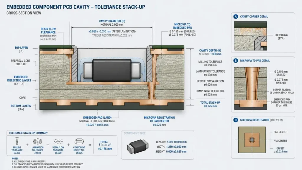
Industrial IoT Embedded PCB Cavity Tolerance Stack-Up Diagram – Hongda Circuit
Cavity tolerance should be evaluated as a tolerance stack involving component dimensions, placement accuracy, cavity fabrication, layer registration, lamination movement, and design clearance.
A nominal CAD cavity is not enough.
Consider a simplified example:
- Component dimensional tolerance: ±0.05 mm
- Placement tolerance: ±0.05 mm
- Cavity fabrication tolerance: ±0.05 mm
- Registration/process allowance: ±0.05 mm
The accumulated process envelope can approach 0.20 mm across these independent contributions if treated conservatively.
The correct design margin depends on how the tolerances are defined and statistically combined, but the engineering lesson is straightforward:
Do not dimension an embedded cavity from nominal component dimensions alone.
The manufacturing question
Before releasing the design, ask the PCB manufacturer:
- What cavity tolerance is qualified in production?
- What placement accuracy is demonstrated?
- What registration accuracy is available between the cavity and subsequent via layers?
- How does lamination movement affect the finished geometry?
- What minimum clearance is recommended around this component?
- Can the supplier provide a representative cross‑section?
This is where DFM becomes more valuable than a generic “design rule” document.
What Manufacturing Problems Occur During Industrial IoT Embedded PCB Production?
The most significant manufacturing risks are component shift, cavity dimensional variation, resin voids, incomplete filling, lamination stress, layer registration errors, microvia defects, copper imbalance, warpage, and hidden internal defects.
The difficult part is that several of these defects can remain invisible from the finished PCB surface.
Manufacturing Pain Point 1 — Component Shift
If an embedded component moves during placement or lamination, subsequent microvias may miss their intended pads.
A small positional error can therefore become an electrical failure several process steps later.
Manufacturing Pain Point 2 — Resin Voids
Insufficient or uncontrolled resin flow can leave voids around embedded structures.
Potential consequences include:
- localized mechanical weakness
- moisture pathways
- thermal resistance increase
- delamination risk
- dimensional instability
Manufacturing Pain Point 3 — Lamination Pressure
The embedded component changes the local physical structure of the PCB.
The press cycle must therefore be compatible with:
- component dimensions
- resin system
- copper distribution
- cavity geometry
- dielectric thickness
- required void control
Manufacturing Pain Point 4 — Copper Imbalance
Large copper areas adjacent to sparse routing areas can produce non‑uniform behavior during fabrication and lamination.
For compact Industrial IoT boards, this can become significant because the embedded component area may introduce unusual internal copper patterns.
Manufacturing Pain Point 5 — Hidden Defects
A surface‑mounted resistor can be visually inspected.
A buried resistor cannot.
That changes the inspection strategy fundamentally.
How Do Lamination and Resin Flow Affect Embedded Industrial IoT PCBs?
Lamination determines whether the embedded component becomes mechanically stable inside the PCB, and resin flow determines whether the surrounding dielectric is adequately filled without creating voids, excessive stress, or dimensional distortion.
This is one area where an experienced manufacturer can identify problems before the first production lot.
A useful way to think about the process is:
Component geometry → cavity volume → resin volume → pressure/temperature profile → final dielectric structure
If the component occupies too much local volume, the available resin may be insufficient.
If too much resin accumulates, local thickness and registration may shift.
If copper distribution is asymmetric, the press behavior may also become less predictable.
Engineering checkpoint
For every new embedded design, review:
- component thickness
- cavity depth
- cavity width/length
- dielectric thickness
- resin content
- copper balance
- press cycle
- expected final thickness
- warpage requirement
The objective is not simply “void‑free lamination.”
The objective is repeatable internal geometry after lamination.
How Should Microvias Be Designed Around Embedded Components?
Microvia design around embedded components must account for target‑pad diameter, dielectric thickness, laser diameter, copper thickness, registration tolerance, plating thickness, and the chosen stacked or staggered structure.
A representative planning range for an HDI Industrial IoT board might use microvia openings around 75–150 µm, depending on dielectric thickness and fabrication capability.
However, a 100 µm laser opening should never be evaluated in isolation.
The engineer should review:
Laser opening / dielectric thickness / target pad / capture pad / copper thickness / plating / registration
Stacked microvias
Stacked microvias can provide vertical interconnection through build‑up layers.
They are attractive when routing density is high.
But the interface between stacked structures requires tight process control.
Staggered microvias
Staggered structures can reduce some stacking‑related process complexity by shifting the microvia position between layers.
Copper‑filled microvias
Copper filling can create a planarized structure suitable for subsequent build‑up processing and selected via‑in‑pad architectures.
IPC’s board‑design standards include HDI and microvia‑related design guidance, while IPC‑A‑600 includes acceptance guidance for internally observable PCB conditions and microvia target landing features.
How Should Thermal Management Be Designed for Industrial IoT Embedded PCBs?
Thermal management should be designed from the heat source to the final heat sink, considering component power, copper area, thermal vias, dielectric thermal resistance, internal planes, enclosure conditions, and ambient temperature.
Embedding does not automatically improve thermal performance.
In some structures it can actually make heat removal more difficult.
For a heat‑generating device, engineers should define a thermal path such as:
Component → copper → thermal via → internal plane → heat spreader/chassis
Example thermal calculation
The basic relationship is:
P = I²R
For a 2 A path with 50 mΩ resistance:
P = 2² × 0.05 = 0.20 W
That 0.20 W may appear small.
But inside a sealed industrial enclosure with limited airflow, several local heat sources can accumulate.
For a 5 W embedded power device with an effective junction‑to‑case or junction‑to‑board thermal resistance of 10°C/W, the approximate temperature rise would be:
ΔT ≈ 5 W × 10°C/W = 50°C
This illustrates why thermal design must be performed at the system level.
The actual thermal resistance must come from the component, PCB construction, copper geometry and thermal boundary conditions.
How Should Industrial Ethernet and High‑Speed Signals Be Routed?
High‑speed Industrial IoT interfaces should be routed using controlled impedance, continuous return paths, appropriate reference planes, matched differential geometry, controlled via transitions, and a material system appropriate to the operating frequency and loss budget.
Industrial Ethernet may coexist with:
- DC/DC converters
- relay drivers
- motors
- sensors
- analog front ends
- isolated interfaces
That creates an EMC challenge.
Embedding selected components can reduce certain interconnect lengths, but it does not eliminate the need for good high‑speed layout.
Critical parameters include:
- characteristic impedance
- differential impedance
- insertion loss
- return loss
- crosstalk
- dielectric Dk/Df
- copper roughness
- via discontinuity
- return‑current path
- connector transition
For higher‑speed Industrial IoT designs, the relevant frequency behavior is determined by the signal edge rate, not merely the nominal data‑rate label.
This distinction matters when deciding whether a standard FR‑4 stack‑up is adequate or whether a lower‑loss material should be evaluated.
How Should EMC and EMI Be Managed in an Embedded Industrial IoT PCB?
EMC performance depends on the complete current‑return and field‑control architecture, including grounding, reference planes, filtering, shielding, component placement, differential routing, power conversion and enclosure design.
An embedded capacitor may reduce the physical path between a load and its decoupling element.
That can be beneficial.
But the board can still fail EMC testing if:
- return paths are interrupted
- switching nodes are too large
- high‑current loops are excessive
- noisy and sensitive circuits share poor reference structures
- connector filtering is poorly positioned
- shielding is incomplete
Industrial EMC scenario
Imagine a sensor board mounted 50 mm from a motor driver.
The sensor operates at a low signal level while the motor drive generates strong switching transients.
Simply embedding the sensor’s decoupling capacitor does not solve the system problem.
The PCB must also manage:
source → coupling path → victim → return path
That is the engineering framework we recommend using during layout review.
How Should Industrial IoT Embedded PCBs Be Tested for Reliability?
Reliability validation should test both the PCB structure and the embedded component interfaces under the actual electrical, thermal, mechanical, and environmental conditions expected during service.
A conventional visual inspection strategy is insufficient for many embedded structures.
A practical validation matrix can include:
| Test / Inspection | Primary Purpose |
|---|---|
| AOI | Surface fabrication defects |
| 2D/3D X‑ray | Internal component and interconnection inspection |
| Cross‑section | Cavity, copper, dielectric and microvia analysis |
| Electrical continuity | Open/short detection |
| Flying probe / ICT | Electrical verification depending on design |
| Thermal cycling | Temperature‑induced stress |
| Mechanical/vibration testing | Structural integrity |
| Moisture/environmental testing | Environmental durability |
| Microvia evaluation | Interconnection reliability |
| Solderability testing | Applicable external assembly interfaces |
| Impedance testing | High‑speed interconnect verification |
The actual test matrix should be agreed between the product owner and manufacturer based on the product’s qualification requirements.
IPC‑7092 includes component robustness, test‑method correlation, material requirements, cost analysis and product‑safety considerations; IPC’s standards framework also identifies IPC‑TM‑650, IPC‑A‑600 and IPC‑6012 among relevant PCB quality and performance references.
How Can DFM Prevent Industrial IoT Embedded PCB Failures?
DFM should begin before quotation and should verify whether the electrical design can be converted into a stable production process with controlled tolerances, acceptable yield, inspectability, and scalable manufacturing cost.
This is where the difference between prototype capability and production capability becomes important.
A supplier may successfully manufacture one prototype while still having difficulty achieving stable volume yield.
Our recommended DFM sequence
1. Review component geometry Check:
- length
- width
- thickness
- termination
- temperature rating
- electrical rating
2. Review cavity Check:
- length
- width
- depth
- corner geometry
- clearance
3. Review registration Check:
- cavity‑to‑pad
- pad‑to‑microvia
- layer‑to‑layer
- build‑up alignment
4. Review lamination Check:
- dielectric thickness
- resin availability
- copper balance
- component height
- final board thickness
5. Review electrical access Check:
- microvia
- via‑in‑pad
- stacked/staggered structures
- impedance
- return path
6. Review inspection Ask:
How will we detect a defect after this component is buried?
If there is no credible inspection method, the design deserves another review.
What Are the Most Common Industrial IoT Embedded PCB Design Mistakes?
The most common mistakes are treating embedding as a packaging shortcut, designing cavities from nominal dimensions, ignoring lamination movement, placing heat sources without a thermal path, overlooking repairability, and specifying advanced features without confirming the manufacturer’s qualified process window.
Mistake 1: Embedding everything
Not every SMT component needs to be buried.
Embedding should be selective.
Mistake 2: Optimizing only board area
A 10% area reduction is not automatically valuable if it increases manufacturing cost or reduces field repairability.
Mistake 3: Ignoring component replacement
Embedded components are difficult to access after lamination.
For field‑service equipment, this can be a major lifecycle consideration.
Mistake 4: Using a generic microvia rule
A microvia diameter without dielectric thickness and target‑pad information is not a complete engineering specification.
Mistake 5: Treating IPC as a substitute for product qualification
IPC standards provide important design and manufacturing guidance, but the product owner still needs to define the actual environmental, electrical and reliability requirements.
Mistake 6: Comparing suppliers only by unit price
The correct comparison is:
Unit price + tooling + engineering + yield + scrap + testing + logistics + lifecycle cost
rather than piece price alone.
How Does an Embedded Industrial IoT PCB Compare With a Conventional SMT PCB?
Embedded architecture offers higher integration density and can recover surface area, but conventional SMT remains simpler to manufacture, inspect, repair, and modify. The better architecture depends on the product’s space, performance, volume, reliability, and service requirements.
| Factor | Embedded Industrial IoT PCB | Conventional SMT PCB |
|---|---|---|
| Surface‑area efficiency | High | Moderate |
| Component accessibility | Low | High |
| Repairability | More difficult | Easier |
| Manufacturing complexity | Higher | Lower |
| Hidden‑feature inspection | Required | Less extensive |
| Routing density | Potentially higher | Moderate to high |
| Parasitic path | Can be reduced | Often longer |
| Thermal design | Application‑dependent | More straightforward |
| DFM requirement | High | Moderate |
| Prototype flexibility | Lower | Higher |
| Integration density | High | Moderate to high |
| Initial engineering effort | Higher | Lower |
The correct conclusion is not that embedding replaces SMT.
It is that embedded components provide another integration layer for designs where surface mounting creates a measurable system constraint.
How Can Industrial IoT Embedded Components Improve Board‑Level Power Integrity?
Embedded capacitive structures can place capacitance closer to power‑consuming devices, potentially reducing interconnect inductance and improving local high‑frequency decoupling, but the complete power‑distribution network must still be modeled and validated.
A simplified PDN model can be expressed as:
ZPDN = Vnoise / Itransient
For example, if a transient load changes by:
ΔI = 0.5 A
and the allowable transient voltage deviation is:
ΔV = 25 mV
then the target PDN impedance is approximately:
ZPDN ≤ 25 mV / 0.5 A = 50 mΩ
This is a design example, not a universal Industrial IoT requirement.
It demonstrates the correct engineering approach:
Define allowable noise → calculate target impedance → design capacitance/planes → validate the actual PDN.
That is more meaningful than simply saying “embedded capacitors improve power integrity.”
How Should Materials Be Selected for Industrial IoT Embedded PCBs?
Material selection should match the application’s temperature, frequency, mechanical stress, dielectric requirements, moisture exposure, copper structure, and expected production volume.
Standard Industrial IoT applications
Many industrial controllers and sensors can be designed around qualified FR‑4 systems.
Higher‑temperature applications
High‑Tg laminates may be considered when the product experiences elevated operating or process temperatures.
High‑speed communication
Low‑loss materials may become appropriate when the signal loss budget cannot be achieved with the selected conventional material.
Embedded resistor structures
Dedicated resistive materials may be required depending on the resistance range, tolerance, power and fabrication architecture.
Dielectric selection
For controlled‑impedance and embedded‑capacitor structures, dielectric thickness and dielectric constant must be treated as part of the electrical design rather than merely as mechanical thickness.
The current IPC standards ecosystem includes dedicated material and performance standards alongside embedded‑component and HDI guidance.
What 2026 PCB Manufacturing Technologies Matter for Industrial IoT Embedded PCBs?
The most immediately useful 2026 technologies are advanced HDI, laser microvias, fine‑line/mSAP fabrication, improved imaging and registration, automated inspection, digital traceability, and increasingly integrated PCB‑package manufacturing processes.
The technology direction is becoming increasingly clear:
HDI → fine‑line → mSAP → embedded components → embedded die → advanced packaging
Würth Elektronik currently describes embedding approaches including SOLDER.embedding, MICROVIA.embedding, FLIP‑CHIP.embedding and COPPER.embedding, reflecting how component integration is moving beyond simple passive placement.
mSAP and fine‑line processing
For compact Industrial IoT devices, mSAP can become useful when conventional subtractive etching becomes restrictive for fine geometry.
However, a supplier’s headline line/space number is not sufficient.
Procurement should ask:
- At what copper thickness?
- On which layer?
- With what registration?
- At what panel size?
- At what production yield?
- With what inspection method?
LDI
LDI can support fine‑line imaging and registration control without relying on conventional phototools.
For embedded structures, registration matters because the manufacturing chain contains multiple coordinate‑dependent operations:
cavity → component → pad → microvia → routing
Laser drilling
UV and CO₂ laser systems support microvia formation in HDI build‑up structures.
The actual process window depends on:
- dielectric thickness
- resin composition
- copper thickness
- laser wavelength
- pulse energy
- target‑pad structure
- required hole quality
Automated inspection
As internal structures become harder to inspect visually, AOI, X‑ray, cross‑section analysis and electrical testing become increasingly important.
The trend is therefore not simply toward “more advanced equipment.”
It is toward more measurable manufacturing processes.
How Should Buyers Qualify an Industrial IoT Embedded Component PCB Manufacturer?
Buyers should qualify the supplier based on demonstrated embedded‑component process capability, DFM engineering, cavity control, lamination, HDI/microvia manufacturing, inspection, reliability validation, traceability, and the ability to transfer a prototype process into stable production.
Do not begin with:
“What is your PCB price?”
Begin with:
“Can you manufacture this structure repeatedly within the required tolerance and reliability window?”
Supplier qualification checklist
| Qualification Item | What Procurement Should Verify |
|---|---|
| Embedded passive capability | Actual production examples |
| Embedded active capability | Process scope and limitations |
| Cavity fabrication | Qualified dimensional tolerance |
| Component placement | Demonstrated accuracy |
| Lamination | Process control and void management |
| HDI | Microvia structure and capability |
| mSAP | Qualified line/space and copper thickness |
| Registration | Layer‑to‑layer capability |
| X‑ray | Internal inspection capability |
| Cross‑section | Microsection analysis |
| Electrical testing | Continuity/isolation/test coverage |
| Reliability | Relevant environmental validation |
| Traceability | Lot/process records |
| DFM | Engineering review before production |
| Prototype‑to‑volume | Process transfer evidence |
Sierra Circuits, for example, publicly emphasizes industrial PCB DFM/DFA, inspection, electrical testing, documented quality records and manufacturing capabilities; its industrial PCB page also provides specific capability figures such as layer count, board thickness, impedance tolerance and laser‑drilling limits.
The important lesson is not to copy another manufacturer’s capability numbers.
It is to ask every supplier for their own qualified production capability.
What Should Be Included in an Industrial IoT Embedded PCB RFQ?
An Industrial IoT embedded PCB RFQ should contain the complete electrical design data plus component dimensions, embedding locations, environmental requirements, reliability targets, testing requirements, and production volume.
Minimum RFQ package
PCB data
- Gerber / ODB++
- PCB dimensions
- layer count
- stack‑up
- finished thickness
- copper thickness
- surface finish
- impedance requirements
Embedded‑component data
- component manufacturer
- part number
- length
- width
- thickness / Z‑height
- electrical rating
- tolerance
- embedding location
- cavity drawing
- termination information
Application data
- Industrial IoT application
- operating temperature
- storage temperature
- humidity
- vibration
- expected service life
- electrical environment
- communication interfaces
Production data
- prototype quantity
- annual volume
- target production quantity
- required delivery schedule
Quality data
- inspection requirements
- electrical testing
- X‑ray
- cross‑section
- thermal cycling
- reliability requirements
- applicable IPC requirements
This information allows the supplier to quote the actual manufacturing problem rather than a simplified PCB commodity.
How Can Industrial IoT Embedded PCB Cost Be Controlled?
Cost is best controlled by optimizing the embedding architecture during DFM rather than reducing material or process requirements after the design has already been released.
A useful total‑cost model is:
TCO = PCB fabrication + components + assembly + tooling + testing + scrap + logistics + engineering + field‑service cost
Cost driver 1 — Layer count
Additional layers increase:
- laminate consumption
- lamination cycles
- drilling
- plating
- imaging
- inspection
Cost driver 2 — Embedded component count
More embedded devices generally increase placement and process complexity.
Cost driver 3 — Cavity complexity
Multiple cavity depths or unusual shapes may increase tooling and process‑control requirements.
Cost driver 4 — Microvia density
More laser drilling and more complex interconnection structures can increase process time and inspection requirements.
Cost driver 5 — Yield
This is often underestimated.
Consider two suppliers:
Supplier A
- Unit price: $10
- Yield: 95%
Supplier B
- Unit price: $8.50
- Yield: 75%
The cheaper nominal price does not automatically produce the lower manufacturing cost.
This is why we recommend asking for production yield for comparable embedded structures, not just asking whether the supplier can make the design.
What Is the Best Design Strategy for a Reliable Industrial IoT Embedded PCB?
The most reliable strategy is selective embedding combined with controlled stack‑up design, conservative tolerance allocation, appropriate HDI structures, validated lamination, thermal analysis, hidden‑structure inspection, and application‑specific reliability testing.
A practical design sequence is:
Application requirements ↓ Component selection ↓ Embedding candidates ↓ Electrical analysis ↓ Mechanical/tolerance analysis ↓ Thermal analysis ↓ Stack‑up ↓ DFM ↓ Prototype ↓ Cross‑section + inspection ↓ Reliability validation ↓ Volume production
This sequence prevents a common mistake: optimizing the PCB layout first and discovering manufacturing limitations later.
What Are Hongda Engineers Looking for During an Industrial IoT PCB Review?
We look first for interactions between embedded structures rather than reviewing each feature independently.
At Shenzhen Hongda Circuit Technology Co., Ltd., our engineering review focuses on several practical interfaces.
Component → Cavity
Does the cavity provide enough process margin?
Cavity → Lamination
Is there adequate dielectric and resin around the component?
Component → Microvia
Can the subsequent interconnection land reliably on the intended pad?
Copper → Thermal Path
Does the copper structure provide a realistic heat path?
Signal → Return Path
Does the embedded architecture preserve the intended electrical reference?
Prototype → Production
Can the same process window be maintained at volume?
One recurring engineering lesson is that a design can be electrically correct and still be manufacturing‑unstable.
For example, a cavity may look completely acceptable in CAD when the component is represented at nominal dimensions. Once component tolerance, placement error, cavity fabrication tolerance, registration allowance and lamination movement are considered together, the available process margin can become much smaller.
That is why we prefer to review the tolerance stack before tooling.
Another practical lesson is that microvia diameter should never be specified as an isolated number. The dielectric thickness, target pad, copper thickness, laser process and plating structure must be reviewed as one interconnection system.
These are small engineering details, but they are often what separates a prototype that works once from a production process that works repeatedly.
How Can Shenzhen Hongda Circuit Technology Support Industrial IoT Embedded PCB Projects?
Shenzhen Hongda Circuit Technology Co., Ltd. can support Industrial IoT embedded PCB projects through advanced multilayer, HDI, laser‑drilling, fine‑line/mSAP, automated inspection, and engineering‑oriented manufacturing processes.
Our published manufacturing portfolio includes:
- LDI fine‑line imaging
- UV/CO₂ laser drilling
- Advanced laser processing
- HDI microvia manufacturing
- mSAP fine‑line PCB fabrication
- Automated plating
- AOI inspection
- X‑ray inspection
- High‑density multilayer PCB manufacturing
The important point is how these technologies are combined.
An Industrial IoT embedded PCB is not manufactured by one machine.
It requires a controlled chain:
Material selection → Internal circuit fabrication → Cavity formation → Component placement → Lamination → Laser drilling → Plating → Fine‑line routing → Surface finishing → AOI/X‑ray → Electrical testing → Final inspection
Our engineering objective is to identify the manufacturing risks before they become production defects.
For Industrial IoT projects, we recommend that customers provide the Gerber/ODB++ files, BOM, stack‑up, component Z‑height, embedding locations, environmental requirements, quantity, and reliability/test requirements during the quotation stage.
This allows the engineering team to evaluate manufacturability before production release.
What Questions Should Procurement Teams Ask Before Ordering an Industrial IoT Embedded PCB?
Procurement should ask for measurable manufacturing evidence rather than relying on general statements such as “high precision,” “advanced technology,” or “industrial‑grade quality.”
Use these questions during supplier qualification:
- What embedded components have you manufactured in production?
- What cavity dimensional tolerance can you qualify repeatedly?
- What component placement accuracy can you demonstrate?
- What microvia diameter and aspect ratio are qualified for this dielectric thickness?
- Can you provide representative cross‑section data?
- How are internal embedded structures inspected after lamination?
- What is the production yield for comparable embedded designs?
- Can your prototype process be transferred to volume production?
- How do you control lamination movement and component shift?
- Which reliability tests can you support?
- How do you manage process traceability?
- Can engineering review the design before quotation?
A capable supplier should answer with process capability, inspection methodology and engineering evidence, not only marketing terminology.
What Are the 5 Most Important Procurement FAQs About Industrial IoT Embedded Component PCBs?
What files are required to quote an Industrial IoT embedded component PCB?
Provide the Gerber or ODB++ manufacturing data, BOM, stack-up, PCB dimensions, embedded-component locations, component dimensions/Z-height, cavity information, material requirements, copper thickness, via structure, quantity, application conditions, and required testing.
For complex projects, providing the component datasheets and mechanical drawing is strongly recommended.
Are embedded component PCBs suitable for harsh industrial environments?
They can be suitable when the PCB material system, embedded component, interconnection structure, lamination process and environmental qualification are selected for the actual application.
For a product specified at −40 to +85°C, for example, the entire structure should be evaluated across that temperature range rather than qualifying only the surface-mounted components.
The same principle applies to humidity, vibration, contamination and electrical transients.
Is an Industrial IoT embedded PCB more expensive than a conventional SMT PCB?
Usually, the fabrication and engineering process is more complex, particularly when cavities, HDI, microvias, special materials or embedded active devices are involved.
However, the system-level economics can be different.
Embedding may reduce:
surface assembly count
board footprint
enclosure volume
selected routing complexity
selected interconnection length
The correct comparison is therefore total cost of ownership, not bare PCB price.
What is the biggest manufacturing risk in an embedded Industrial IoT PCB?
For many designs, the highest risks are associated with the interaction between component placement, cavity tolerance, lamination, internal registration and subsequent microvia formation.
A hidden defect can survive several manufacturing stages before it becomes detectable.
That is why early DFM, X-ray inspection, cross-section analysis and appropriate electrical testing are valuable.
How should I choose an Industrial IoT embedded PCB manufacturer?
Choose a supplier that can demonstrate the complete manufacturing chain required by your design.
At minimum, evaluate:
Embedded-component experience + cavity capability + lamination + HDI/microvia + fine-line processing + inspection + electrical testing + reliability validation + traceability + DFM support
Do not qualify a supplier solely from its maximum advertised line/space or lowest quotation.
Ask for evidence from a comparable production structure.
Final Engineering Perspective: When Does Embedded PCB Technology Make Sense for Industrial IoT?
Embedded Component PCB technology makes the most sense when it solves a measurable Industrial IoT system constraint that conventional SMT cannot address efficiently, particularly severe space limitations, routing congestion, selected high-speed interconnect requirements, or integration-density targets.
The technology should not be selected simply because embedding is more advanced.
A successful Industrial IoT embedded PCB balances:
Miniaturization
- Electrical performance
- Thermal behavior
- EMC
- Mechanical reliability
- Manufacturing yield
- Inspection
- Repairability
- Total cost
The most important engineering question is therefore not:
“Can this component be embedded?”
It is:
“What system problem does embedding solve, and can the resulting structure be manufactured repeatedly within the required electrical, mechanical, thermal and reliability limits?”
That is the standard we recommend using when evaluating an Industrial IoT Embedded Component PCB project.
Shenzhen Hongda Circuit Technology Co., Ltd. supports advanced PCB manufacturing for customers requiring embedded components, HDI, microvias, fine-line/mSAP structures and high-density multilayer construction.
For an engineering review, prepare your Gerber/ODB++, BOM, stack-up, embedded-component specifications, PCB dimensions, environmental requirements, prototype quantity and annual volume.
Email: pcb@pcbkr.com
Website: www.pcbkr.com
About Author
David Chen https://www.linkedin.com/in/pcbcoming
David Chen boasts an extensive professional background in PCBA manufacturing, PCBA testing, and PCBA optimization, with specialized expertise in high-precision PCBA fault analysis and rigorous PCBA reliability testing. The author has worked with high-layer-count server PCB fabrication, ultra-low-loss backplane stackups, and thermo-mechanical reliability optimization for AI infrastructure projects involving 112G and 224G PAM4 architectures. Skilled in complex circuit design and cutting-edge advanced PCB manufacturing processes, he delivers solutions that elevate product durability and performance across industrial applications. His technical articles focusing on PCBA manufacturing workflows and testing methodologies are widely cited by industry peers, research institutions, and technical platforms, solidifying his reputation as a recognized technical authority in the global circuit board manufacturing sector.