High-Frequency Embedded PCB Manufacturer | Prototype to Volume
High-Frequency Embedded Component PCB is a specialized circuit board solution that integrates embedded capacitors, resistors, inductors and other passive components as well as active devices, while adopting low-loss dielectric materials, controlled impedance design, microvia technology and precision lamination processes for high-frequency signal scenarios. Different from conventional miniaturized PCB fabrication that merely regards component embedding as a simple size-reduction technique, the core of high-frequency embedded component PCB manufacturing lies in systematic RF process control. It takes multiple core parameters as a complete RF manufacturing system for unified precision management, including dielectric constant (Dk) and dissipation factor (Df) of materials, copper surface roughness, dielectric layer thickness, embedded component placement accuracy, via hole geometric dimensions and board cavity structure. This integrated manufacturing mode effectively eliminates signal attenuation, impedance mutation and parasitic interference caused by discrete component welding and traditional circuit board processing defects, ensuring excellent high-frequency signal transmission performance, stability and consistency of the PCB, which is highly suitable for high-speed communication, radio frequency sensing and other high-precision electronic fields.
What Makes an Embedded Component PCB Suitable for High‑Frequency Applications?
A high‑frequency embedded component PCB is suitable for RF or high‑speed applications when its material system, embedded‑component geometry, transmission‑line structure, vias, copper profile, and manufacturing tolerances are controlled against the actual frequency and signal‑integrity requirements.
A conventional embedded‑component PCB primarily solves space and interconnection‑density problems. A high‑frequency embedded PCB must solve those problems without introducing unacceptable electrical discontinuities.
The engineering chain is therefore:
Frequency → material → stack‑up → component location → transmission line → via transition → manufacturing tolerance → RF verification
This distinction is important because the pillar topic, Embedded Component PCB: Technology, Manufacturing & Procurement Guide, already covers the general technology, embedded structures, HDI, mSAP, inspection, procurement, and supplier evaluation.
The high‑frequency cluster should instead concentrate on the electromagnetic and manufacturing interactions created when embedded components are placed inside an RF/high‑speed PCB.
Typical applications include:
| Application | Typical frequency/data environment | Embedded‑component objective |
|---|---|---|
| Automotive radar | 24–81 GHz | RF miniaturization, controlled parasitics |
| RF front‑end module | MHz–mmWave | Shorter electrical paths |
| Wireless infrastructure | GHz/mmWave | Lower loss and stable impedance |
| AI/server hardware | 56–224G‑class signaling | Power integrity and interconnect density |
| High‑speed computing | Multi‑GHz | Decoupling and reduced loop inductance |
| Compact RF modules | Application‑dependent | Functional density |
For microwave boards, IPC‑6018D specifically covers high‑frequency printed boards with microstrip, stripline, mixed dielectric multilayers, blind/buried vias, metal cores, and boards containing embedded active or passive circuitry and HDI layers.
How Does Embedding Change the Electrical Path at High Frequency?
Embedding can shorten the electrical path between a component and its reference or power structure, reducing the physical loop area and potentially reducing parasitic inductance and capacitance, but the benefit depends strongly on placement, dielectric geometry, via structure, and component construction.
Consider a conventional SMT decoupling capacitor.
The electrical path may include:
IC pad → package → PCB pad → solder joint → via → capacitor → ground via → reference plane
Every additional millimeter and transition contributes electrical parasitics.
With an embedded capacitor, the component can be positioned closer to the power distribution structure:
IC → short internal connection → embedded capacitor → internal reference plane
This can reduce the physical interconnect loop.
However, embedding does not automatically guarantee lower loss or better RF performance.
A poorly positioned embedded component can introduce: ‑ discontinuous reference planes; ‑ excessive via inductance; ‑ cavity‑related impedance discontinuity; ‑ local dielectric‑thickness variation; ‑ component registration errors; ‑ unexpected resonances; ‑ manufacturing‑induced dimensional variation.
The pillar article already identifies reduced parasitic inductance, improved signal integrity, EMI benefits, and higher functional density as important advantages of embedded components.
The high‑frequency question is more specific:
Where exactly is the component placed relative to the RF current path, and what does manufacturing do to that electromagnetic geometry?
That is where high‑frequency embedded PCB engineering becomes substantially more demanding.
Which PCB Materials Should Be Used for High‑Frequency Embedded Components?
Material selection should be based on frequency, Dk stability, Df, copper profile, thermal behavior, dimensional stability, and compatibility with the embedded‑component manufacturing process—not simply on the material’s nominal Dk.
For RF applications, commonly considered material families include: ‑ PTFE‑based materials; ‑ ceramic‑filled PTFE materials; ‑ low‑loss hydrocarbon/ceramic systems; ‑ low‑loss modified epoxy systems; ‑ high‑speed FR‑4 families; ‑ hybrid dielectric constructions.
The correct choice depends on the electrical frequency and the required loss budget.
For example, Rogers reports RO3003 with a nominal Dk of 3.00 ±0.04 and a dissipation factor around 0.0010 at 10 GHz on its product information. Rogers also positions the material for applications including automotive radar and 77 GHz systems.
That does not mean RO3003 is the correct material for every embedded RF PCB.
Instead, the supplier should evaluate:
- Design Dk.
- Process Dk.
- Df at the actual operating frequency.
- Copper roughness.
- Finished dielectric thickness.
- Temperature coefficient of Dk.
- CTE.
- Moisture behavior.
- Lamination compatibility.
- Embedded‑component processing compatibility.
A high‑frequency PCB manufacturer should therefore provide a material datasheet and controlled stack‑up, rather than simply stating “Rogers material available.”
How Do Dk and Df Affect High‑Frequency Embedded PCB Performance?
Dk primarily influences transmission‑line geometry and propagation characteristics, while Df contributes to dielectric loss; both must be evaluated at the relevant frequency and temperature rather than using a generic room‑temperature material value.
For a simplified transmission‑line model, propagation velocity is related approximately to the effective dielectric constant:
v ≈ c / √εeff
where: ‑ v = propagation velocity; ‑ c = speed of light; ‑ εeff = effective dielectric constant.
The practical problem is that Dk is not simply a number printed on a material label.
The effective value depends on: ‑ frequency; ‑ resin content; ‑ glass weave; ‑ copper geometry; ‑ dielectric thickness; ‑ measurement method; ‑ temperature; ‑ local material construction.
At millimeter‑wave frequencies, even small variations can affect phase and impedance.
Rogers, for example, publishes detailed high‑frequency material data and has demonstrated the effect of Dk variation on phase behavior around 77 GHz.
Therefore, a high‑frequency embedded PCB RFQ should specify the material grade and electrical test method, not only “low Dk material.”
How Does Copper Roughness Affect RF and High‑Speed Signal Loss?
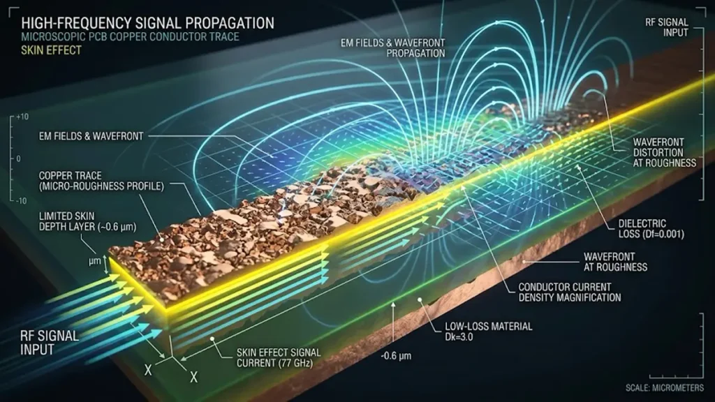
Microscopic Rendering of PCB Copper Roughness and Skin Effect Signal Loss
Copper roughness becomes increasingly important as frequency rises because high‑frequency current concentrates toward conductor surfaces, making the effective electrical path sensitive to conductor topography.
This is particularly important above several GHz and becomes increasingly critical in mmWave applications.
A PCB manufacturer may therefore offer: ‑ standard electrodeposited copper; ‑ low‑profile copper; ‑ very‑low‑profile copper; ‑ rolled copper for selected applications; ‑ reverse‑treated copper systems.
The engineering question is not:
“Is the copper thick enough?”
It is:
“What copper profile was assumed by the RF loss model, and does the manufactured copper match that assumption?”
This distinction matters because a stack‑up simulation based on ideal smooth copper can underestimate actual conductor loss.
Rogers identifies very‑low‑profile copper as a feature of some high‑frequency materials intended to reduce insertion loss.
For Hongda’s RF PCB manufacturing approach, copper profile should therefore be included as part of the controlled RF stack‑up data, rather than being treated only as a fabrication‑material detail. Hongda also publishes high‑frequency capability information concerning low‑profile copper and environmental Dk/Df control.
How Should the Stack‑Up Be Designed Around Embedded Components?
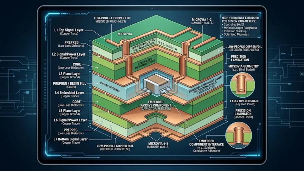
High-Frequency Embedded PCB Stack-Up and Internal Cavity Cross-Section
The stack‑up should be designed from the RF current path outward, with the embedded component, transmission line, reference plane, dielectric thickness, via transition, and thermal structure considered together.
A useful engineering sequence is:
RF layer → dielectric → reference plane → embedded component → power/ground structure → HDI transition
The most important parameters include:
| Parameter | Engineering concern |
|---|---|
| Dielectric thickness | Impedance and field distribution |
| Dk | Trace geometry and propagation |
| Df | Dielectric loss |
| Copper thickness | Resistance and manufacturing geometry |
| Copper roughness | High‑frequency conductor loss |
| Trace width | Impedance |
| Trace spacing | Crosstalk |
| Via diameter | Discontinuity and manufacturability |
| Via stub | Reflection |
| Component position | Parasitic path |
| Cavity geometry | Local electromagnetic discontinuity |
| Reference‑plane continuity | Return‑current integrity |
The original pillar already discusses stack‑up design, cavity dimensions, thermal considerations, signal integrity, and DFM.
The high‑frequency cluster should go further by asking:
What happens to the RF field when the embedded component is introduced into that stack‑up?
That is the engineering distinction between a generic embedded PCB and a high‑frequency embedded PCB.
How Should Embedded Capacitors and Resistors Be Positioned for RF Performance?
Embedded passive components should be positioned according to electrical function rather than simply available physical space, with the shortest practical connection to the power, ground, RF, or matching structure they serve.
For example, an embedded capacitor used for high‑frequency decoupling should normally be placed close to the electrical region where its high‑frequency current is required.
The objective is to minimize: ‑ connection length; ‑ via count; ‑ loop area; ‑ uncontrolled inductance; ‑ unnecessary layer transitions.
For RF matching networks, component placement becomes even more sensitive.
A small physical displacement can alter: ‑ transmission‑line length; ‑ local impedance; ‑ coupling; ‑ parasitic capacitance; ‑ parasitic inductance; ‑ phase.
Therefore, the PCB fabrication drawing should define component position tolerance rather than assuming that an embedded component will automatically remain centered inside its cavity.
How Do Cavities Affect Impedance and Electromagnetic Behavior?
An embedded‑component cavity changes the local dielectric and mechanical structure, so its width, depth, corner geometry, registration, resin fill, and component position can all influence RF behavior.
The manufacturing sequence may involve:
- Inner‑layer fabrication.
- Cavity formation.
- Component placement.
- Component fixation.
- Sequential lamination.
- Outer‑layer formation.
- Laser drilling.
- Microvia metallization.
- Surface finishing.
- Inspection and electrical verification.
The pillar page describes cavity formation, component placement, sequential lamination, laser drilling, copper filling, and HDI integration as interconnected manufacturing stages.
The high‑frequency problem is that cavity geometry is part of the RF structure.
Manufacturing variation can produce: ‑ cavity depth variation; ‑ component offset; ‑ resin voids; ‑ local dielectric‑thickness variation; ‑ copper‑plane deformation; ‑ lamination‑induced movement.
A cavity that is mechanically acceptable may therefore still require electrical evaluation.
How Should Microvias and Via Transitions Be Controlled?
Microvias should be designed and manufactured as controlled RF discontinuities, with via diameter, pad size, depth, capture geometry, plating, stub length, and reference‑plane transition all considered together.
HDI microvias are particularly useful when an embedded component must connect to outer or inner routing layers without consuming large board area.
Typical structures may include: ‑ 1+N+1; ‑ 2+N+2; ‑ stacked microvias; ‑ staggered microvias; ‑ blind vias; ‑ buried vias; ‑ hybrid via structures.
But smaller does not always mean electrically better.
A poorly designed via can introduce: ‑ excess capacitance; ‑ inductance; ‑ impedance discontinuity; ‑ resonance; ‑ plating reliability problems; ‑ registration sensitivity.
The manufacturing process must also control: ‑ laser energy; ‑ dielectric ablation; ‑ target alignment; ‑ desmear; ‑ copper seed; ‑ electroplating; ‑ via filling; ‑ cross‑section quality.
IPC‑6018D explicitly includes high‑frequency boards using blind and buried vias and HDI structures within its scope.
When Should mSAP Be Used for High‑Frequency Embedded PCB Manufacturing?
mSAP becomes attractive when the embedded high‑frequency design requires fine‑line geometries, high routing density, or substrate‑like interconnection features that are difficult to maintain economically with conventional subtractive etching.
The mSAP process generally builds fine copper features by:
seed copper → photoresist patterning → selective copper plating → resist stripping → controlled seed‑layer removal
Its advantage is not simply “smaller traces.”
It can provide greater control over: ‑ fine‑line geometry; ‑ conductor width; ‑ conductor spacing; ‑ dense BGA escape routing; ‑ substrate‑like interconnect regions.
Hongda’s published manufacturing information describes mSAP capability including 8/8 µm‑class processing and substrate‑oriented fine‑line structures. These should be understood as company‑specific capability claims and should be confirmed against the exact stack‑up, copper thickness, panel size, and production quantity.
For a high‑frequency embedded PCB, the more important question is:
Can the manufacturer maintain the required RF geometry consistently at production volume?
That is more valuable than advertising the smallest theoretical line/space.
How Should Lamination Be Controlled Around Embedded Components?
Lamination must control component position, dielectric thickness, resin flow, cavity filling, pressure, temperature, and registration because these parameters can directly modify both mechanical reliability and RF geometry.
This is one of the most difficult parts of embedded PCB production.
During lamination, several variables interact: ‑ copper distribution; ‑ resin flow; ‑ component thickness; ‑ cavity dimensions; ‑ prepreg thickness; ‑ temperature profile; ‑ pressure profile; ‑ material CTE; ‑ board symmetry.
A component can be correctly positioned before lamination and shift after pressing.
Likewise, the cavity can be dimensionally correct before pressing but experience local resin movement during the lamination cycle.
For high‑frequency structures, this matters because a change in dielectric thickness can change controlled impedance.
The manufacturing objective is therefore not simply:
“No delamination.”
It is:
“No unacceptable dimensional or dielectric change after the complete thermal‑mechanical manufacturing cycle.”
What Are the Most Difficult Manufacturing Problems in High‑Frequency Embedded PCBs?
The most difficult problems are usually not individual processes but interactions between RF electrical requirements and fabrication tolerances.
High‑Frequency Embedded PCB Manufacturing Pain‑Point Matrix
| Manufacturing variable | Possible electrical consequence | Typical control |
|---|---|---|
| Dielectric thickness | Impedance shift | Thickness measurement |
| Dk variation | Phase/impedance variation | Material control |
| Df variation | Loss variation | Material certification |
| Copper roughness | Insertion‑loss increase | Copper‑profile control |
| Trace‑width variation | Impedance shift | LDI + etch compensation |
| Component offset | Parasitic variation | X‑ray / dimensional inspection |
| Cavity variation | Local RF discontinuity | CMM/optical inspection |
| Via diameter variation | Impedance discontinuity | Microsection |
| Via plating defect | Reliability failure | Cross‑section |
| Via stub | Reflection | Backdrill/design control |
| Lamination movement | Registration error | X‑ray / registration control |
| Resin void | Reliability/RF uncertainty | X‑ray/cross‑section |
| Fine‑line over‑etch | Impedance and yield loss | AOI/etch control |
| Material substitution | RF performance shift | Engineering approval |
This is why a supplier’s generic statement such as “we manufacture high‑frequency PCBs” is not sufficient for a demanding embedded RF design.
The supplier needs to demonstrate control of the complete chain.
How Should 77 GHz Automotive Radar Embedded PCBs Be Manufactured?
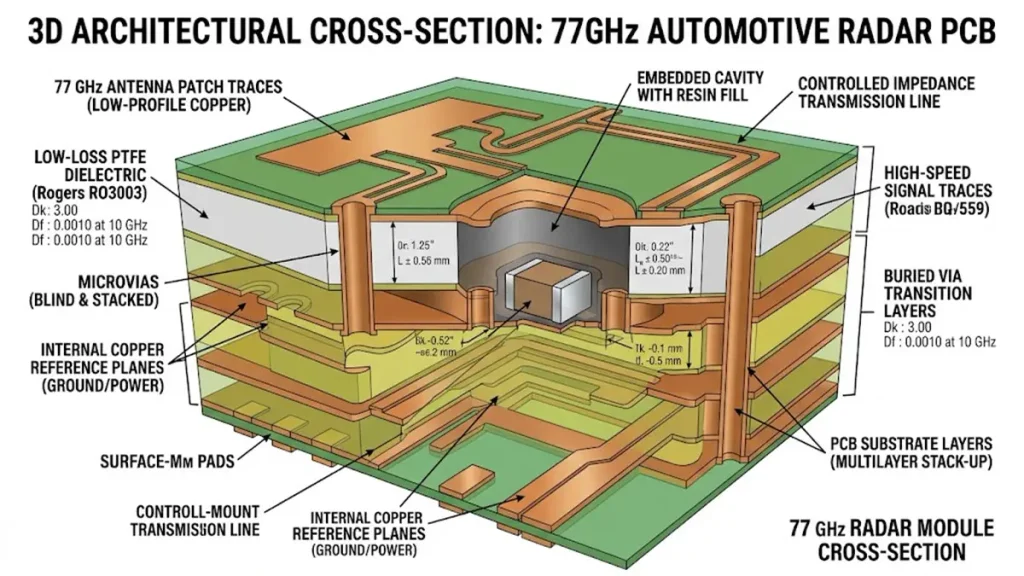
3D Cross-Section Architecture of 77 GHz Automotive Radar Embedded PCB
A 77 GHz embedded radar PCB requires extremely controlled RF material, conductor geometry, reference‑plane continuity, via transitions, component placement, and dimensional stability because small physical variations become electrically significant at millimeter‑wave frequencies.
A typical 77 GHz architecture may contain: ‑ antenna structures; ‑ RF transmission lines; ‑ embedded matching components; ‑ ground‑via fences; ‑ controlled‑impedance transitions; ‑ HDI interconnects; ‑ low‑loss dielectric; ‑ high‑frequency copper.
Rogers specifically identifies RO3003‑family materials for applications including automotive radar and 77 GHz systems, with published Dk/Df characteristics appropriate to high‑frequency design.
The manufacturer therefore needs to understand that 77 GHz is not simply a “higher‑frequency PCB order.”
At this frequency, the PCB itself becomes a significant part of the RF system.
A small variation in: ‑ trace width; ‑ dielectric thickness; ‑ copper profile; ‑ via geometry; ‑ component position;
can change the electromagnetic behavior of the circuit.
How Should 112G and 224G PAM4 Embedded PCBs Be Approached?
For 112G/224G‑class PAM4 systems, embedded components should be evaluated together with channel loss, impedance continuity, return‑current paths, via transitions, power integrity, and package‑to‑board interconnect behavior.
High‑speed digital designs are different from 77 GHz radar, but many manufacturing principles overlap.
For example:
RF/mmWave: material + geometry + phase + loss
High‑speed PAM4: material + geometry + loss + discontinuity + equalization margin
For these applications, the PCB manufacturer should pay particular attention to: ‑ differential‑pair geometry; ‑ dielectric thickness; ‑ copper roughness; ‑ via transitions; ‑ reference‑plane continuity; ‑ connector launches; ‑ backdrilling where required; ‑ impedance coupons; ‑ TDR measurements; ‑ insertion‑loss characterization.
Embedding a capacitor or other passive can improve power integrity, but it must not introduce a new high‑speed discontinuity into the signal path.
How Should High‑Frequency Embedded PCBs Be Tested and Qualified?
Testing should combine conventional PCB inspection with electrical characterization capable of verifying impedance, RF/high‑speed performance, internal structures, and reliability.
A suitable verification program may include:
1. Dimensional inspection
Verify: ‑ board thickness; ‑ cavity dimensions; ‑ component position; ‑ trace geometry; ‑ via dimensions; ‑ registration.
2. AOI
Inspect: ‑ fine‑line defects; ‑ opens; ‑ shorts; ‑ copper‑pattern abnormalities.
3. X‑ray inspection
Particularly useful for hidden: ‑ embedded components; ‑ internal connections; ‑ cavities; ‑ BGA‑related structures; ‑ buried features.
4. Microsection analysis
Cross‑sections can verify: ‑ dielectric thickness; ‑ copper thickness; ‑ microvia formation; ‑ plating; ‑ via filling; ‑ interlayer registration.
5. Controlled‑impedance testing
Use impedance coupons or appropriate measurement structures to verify the manufactured transmission‑line geometry.
6. TDR/VNA testing
Depending on the application, electrical characterization may include: ‑ TDR; ‑ insertion loss; ‑ return loss; ‑ S‑parameters; ‑ frequency‑domain measurements.
7. Reliability testing
The qualification plan may include: ‑ thermal stress; ‑ thermal cycling; ‑ reflow simulation; ‑ humidity exposure; ‑ insulation resistance; ‑ dielectric withstand; ‑ via reliability.
IPC‑6018D establishes qualification and performance requirements for high‑frequency/microwave printed boards and requires procurement documentation to define applicable performance classification and relevant thermal‑stress requirements.
What Manufacturing Data Should a High‑Frequency Embedded PCB Supplier Provide?
A qualified supplier should provide measurable manufacturing evidence rather than relying only on capability statements.
For an RF/high‑speed embedded PCB, request:
| Evidence | Why it matters |
|---|---|
| Material datasheet | Confirms Dk/Df |
| Stack‑up drawing | Confirms physical RF geometry |
| Finished dielectric thickness | Impedance control |
| Copper thickness | Conductor resistance |
| Copper roughness/profile | High‑frequency loss |
| Trace‑width measurement | Impedance consistency |
| Via cross‑section | Interconnect reliability |
| Cavity measurement | Embedded‑component geometry |
| Component‑position data | Electrical/mechanical registration |
| Impedance coupon | Controlled‑impedance verification |
| TDR report | Transmission‑line validation |
| VNA data | RF characterization |
| Reliability report | Production qualification |
| FAI report | First‑production verification |
The original pillar recommends supplier evaluation based on manufacturing capability, DFM, prototyping, quality systems, yield, engineering support, and traceability.
For this high‑frequency cluster, those requirements should be translated into engineering evidence.
How Should Prototype and Mass Production Be Controlled Differently?
Prototype production should prove the stack‑up and manufacturing process, while mass production must prove repeatability and process capability.
A prototype can succeed because engineers closely monitor one panel.
Volume production has a different challenge:
Can the same electrical and dimensional characteristics be reproduced across panels, lots, materials, and production cycles?
The recommended transition is:
Engineering review → DFM → prototype → FAI → qualification → pilot production → volume production
During FAI, record critical‑to‑function parameters such as: ‑ actual dielectric thickness; ‑ trace width; ‑ copper thickness; ‑ cavity dimensions; ‑ component position; ‑ microvia geometry; ‑ impedance; ‑ electrical‑test results.
The FAI dataset then becomes the baseline for production control.
How Should Procurement Teams Compare High‑Frequency Embedded PCB Suppliers?
Procurement should compare suppliers using measurable RF manufacturing evidence, not only price, claimed minimum line/space, or general PCB production capacity.
A practical comparison matrix is:
| Evaluation factor | Supplier A | Supplier B | Supplier C |
|---|---|---|---|
| RF material control | |||
| Dk/Df documentation | |||
| Copper roughness data | |||
| High‑frequency stack‑up engineering | |||
| Embedded component capability | |||
| Cavity registration | |||
| Microvia capability | |||
| mSAP capability | |||
| Controlled impedance | |||
| TDR/VNA capability | |||
| X‑ray inspection | |||
| Microsection | |||
| FAI documentation | |||
| Prototype‑to‑volume transfer | |||
| RF engineering support |
The lowest quotation is not necessarily the lowest total cost.
A supplier that cannot control impedance or embedded‑component registration may create:
prototype failure → redesign → additional tooling → schedule delay → qualification repeat → higher total project cost
For procurement, that is a much more important cost metric than the initial PCB unit price.
What Should Be Included in a High‑Frequency Embedded PCB RFQ?
The RFQ should contain enough electrical, material, structural, and manufacturing information for the supplier to evaluate both feasibility and production risk.
A strong RFQ package should include:
PCB design information
‑ Gerber/ODB++/IPC‑2581 data; ‑ drill files; ‑ stack‑up; ‑ board dimensions; ‑ layer count; ‑ copper thickness.
RF information
‑ operating frequency; ‑ target impedance; ‑ differential impedance if applicable; ‑ insertion‑loss target; ‑ return‑loss target; ‑ maximum allowable phase variation; ‑ RF transmission‑line information.
Material information
‑ approved laminate; ‑ Dk; ‑ Df; ‑ material thickness; ‑ copper type; ‑ copper roughness requirement.
Embedded‑component information
‑ component manufacturer/part number; ‑ component dimensions; ‑ component thickness; ‑ cavity dimensions; ‑ placement tolerance; ‑ internal connection method.
Reliability information
‑ IPC class; ‑ thermal cycling; ‑ reflow profile; ‑ environmental conditions; ‑ application temperature range.
IPC‑6018D specifically emphasizes that procurement documentation must provide sufficient information for the supplier to fabricate and verify the desired high‑frequency board.
How Does Shenzhen Hongda Circuit Technology Approach High‑Frequency Embedded PCB Manufacturing?
Shenzhen Hongda Circuit Technology Co., Ltd. approaches high‑frequency embedded PCB manufacturing as an integrated engineering problem covering materials, HDI, fine‑line fabrication, embedded structures, lamination, inspection, and electrical verification.
The company’s existing embedded‑PCB manufacturing framework covers: ‑ embedded component integration; ‑ cavity structures; ‑ sequential lamination; ‑ laser drilling; ‑ microvias; ‑ copper filling; ‑ HDI; ‑ mSAP; ‑ LDI; ‑ AOI; ‑ X‑ray; ‑ cross‑section analysis; ‑ electrical testing.
For high‑frequency projects, these capabilities should be connected to the customer’s actual RF requirements.
The engineering workflow should therefore be:
Customer RF requirement ↓ Material and Dk/Df review ↓ RF stack‑up analysis ↓ Embedded‑component placement review ↓ Cavity and microvia DFM ↓ Impedance‑controlled fabrication ↓ Prototype ↓ FAI + cross‑section + electrical verification ↓ Qualification ↓ Volume production
This approach is particularly relevant when a design combines high‑frequency materials + embedded components + HDI + fine‑line/mSAP structures.
What Will Define High‑Frequency Embedded PCB Manufacturing ?
The next stage of high‑frequency embedded PCB manufacturing is moving from isolated embedded components toward integrated structures combining embedded actives/passives, HDI, mSAP, substrate‑like interconnects, thermal structures, and data‑driven process control.
The technology direction can be summarized as:
Embedded components + HDI + mSAP + low‑loss materials + advanced packaging + thermal management
The pillar content already identifies this convergence, including embedded dies, mSAP, substrate‑like PCB structures, advanced packaging, and data‑driven manufacturing.
For engineering programs, several developments deserve particular attention:
Embedded active devices
Embedding may expand beyond passive R/C/L devices toward active semiconductor structures and die‑based architectures.
Substrate‑like PCB structures
mSAP and increasingly fine interconnect geometries allow PCB manufacturing to approach packaging‑style density.
Embedded thermal structures
Future embedded designs increasingly need electrical and thermal functions to coexist inside the same board architecture.
AI/high‑speed computing
As signaling rates increase, the PCB becomes increasingly important to the overall channel and power‑integrity budget.
RF/mmWave
Automotive radar, wireless infrastructure, satellite communications, and other mmWave applications place tighter requirements on material stability and conductor geometry.
Data‑driven manufacturing
The long‑term advantage will not simply be the smallest feature a factory can produce once. It will be the ability to measure, record, and reproduce critical parameters across production volume.
What Are the Five Questions Buyers Should Ask Before Choosing a Supplier?
Buyers should ask for measurable manufacturing evidence covering material control, embedded‑component accuracy, RF electrical verification, reliability, and prototype‑to‑volume repeatability.
1. What high‑frequency materials and Dk/Df data can you document?
Ask for the actual material grade, datasheet, frequency range, Dk/Df values, thickness, and approved alternatives.
2. How do you control embedded‑component position after lamination?
Ask for the placement tolerance, cavity tolerance, X‑ray capability, and FAI measurement method.
3. How do you verify high‑frequency impedance?
Ask whether the supplier provides impedance coupons, TDR, VNA or other appropriate electrical characterization.
4. How do you verify hidden microvias and embedded structures?
Ask for X‑ray inspection, microsection capability, plating verification, and reliability‑test documentation.
5. Can you demonstrate prototype‑to‑volume process consistency?
Ask for the manufacturing control plan, FAI report, critical‑dimension records, and process‑change control.
These questions move supplier evaluation from:
“Can you manufacture this PCB?”
to:
“Can you manufacture this electrical structure repeatedly within our RF tolerance?”
That is the more important procurement question.
High‑Frequency Embedded Component PCB RFQ Checklist
Before sending an RFQ, confirm that your engineering package contains: ‑ Operating frequency ‑ Signal type ‑ Target impedance ‑ Differential impedance if applicable ‑ Insertion‑loss requirement ‑ Return‑loss requirement ‑ Approved laminate ‑ Dk/Df requirements ‑ Copper roughness requirement ‑ Finished copper thickness ‑ Stack‑up ‑ Embedded component list ‑ Component dimensions ‑ Cavity dimensions ‑ Component‑position tolerance ‑ Microvia structure ‑ Via/stub requirements ‑ Surface finish ‑ Thermal requirements ‑ IPC performance class ‑ Reliability requirements ‑ Prototype quantity ‑ Expected annual volume ‑ Required inspection reports ‑ FAI requirements
A complete RFQ reduces engineering ambiguity before fabrication begins and makes supplier quotations much easier to compare.
High‑Frequency Embedded Component PCB FAQ
What should I look for in a high-frequency embedded component PCB manufacturer?
Look for a supplier that can demonstrate low-loss material control, controlled impedance, embedded-component registration, cavity fabrication, microvia reliability, RF electrical testing, and prototype-to-volume repeatability—not simply a low minimum line/space specification.
Can embedded component PCBs be manufactured for 77 GHz radar?
Yes, embedded structures can be incorporated into high-frequency radar PCB architectures, but 77 GHz designs require particularly careful control of material properties, conductor geometry, reference planes, component placement, and RF transitions. Rogers identifies suitable high-frequency materials for 77 GHz automotive radar applications.
What line/space and microvia dimensions can a high-frequency embedded PCB manufacturer achieve?
The achievable value depends on copper thickness, dielectric system, panel size, stack-up, feature aspect ratio, plating process, and production volume. A supplier should quote a qualified production capability for the specific construction, rather than applying one minimum number to every PCB.
How are hidden embedded components and internal microvias inspected?
A suitable inspection system can combine X-ray inspection, AOI, dimensional measurement, microsection analysis, electrical testing, and—where appropriate—TDR/VNA characterization. The original pillar specifically identifies AOI, 3D inspection, X-ray, cross-section, and electrical verification as key inspection methods.
What files are required for a high-frequency embedded PCB quotation?
Provide the PCB fabrication data, stack-up, drill information, embedded-component information, material requirements, RF parameters, impedance requirements, cavity drawings, reliability requirements, quantity, and inspection requirements. The more completely the RF and manufacturing requirements are defined, the more meaningful the supplier quotation becomes.
What Is the Real Engineering Challenge of High-Frequency Embedded PCB Manufacturing?
A high-frequency embedded component PCB is not simply a conventional PCB with components placed inside its layers.
Its performance depends on the interaction of:
Material Dk/Df + dielectric thickness + copper roughness + trace geometry + embedded-component position + cavity structure + microvias + lamination + inspection + electrical verification.
The manufacturing challenge is therefore to maintain the electromagnetic design intent after the complete physical manufacturing process.
For procurement teams, the most important supplier question is not:
“What is your smallest line/space?”
It is:
“Can you prove that the critical RF parameters designed into our PCB remain controlled from prototype through volume production?”
For engineering teams developing RF, mmWave, high-speed computing, radar, or compact electronic modules, that distinction can determine whether an embedded PCB is merely manufacturable—or actually performs as designed.
Shenzhen Hongda Circuit Technology Co., Ltd. can evaluate high-frequency embedded PCB projects from the material and stack-up level through embedded-component integration, HDI/microvia fabrication, fine-line/mSAP processing, inspection, prototype validation, and production engineering.
Request a High-Frequency Embedded PCB DFM Review
Request a High-Frequency PCB Prototype Quote
Send Your RF Stack-Up for Engineering Evaluation
Email: pcb@pcbkr.com
Website: www.pcbkr.com
About Author
David Chen https://www.linkedin.com/in/pcbcoming
David Chen boasts an extensive professional background in PCBA manufacturing, PCBA testing, and PCBA optimization, with specialized expertise in high-precision PCBA fault analysis and rigorous PCBA reliability testing. The author has worked with high-layer-count server PCB fabrication, ultra-low-loss backplane stackups, and thermo-mechanical reliability optimization for AI infrastructure projects involving 112G and 224G PAM4 architectures. Skilled in complex circuit design and cutting-edge advanced PCB manufacturing processes, he delivers solutions that elevate product durability and performance across industrial applications. His technical articles focusing on PCBA manufacturing workflows and testing methodologies are widely cited by industry peers, research institutions, and technical platforms, solidifying his reputation as a recognized technical authority in the global circuit board manufacturing sector.