Embedded Component PCB Reliability: Failure Modes, Validation and Manufacturing Controls
Embedded component PCB reliability is controlled by the complete embedded structure—not the component alone. reliable production requires coordinated cavity geometry, CTE-aware materials, controlled lamination, laser microvias, copper interface quality, electrical monitoring, cross-section analysis and application-specific thermal-mechanical validation.
This article expands the original reliability framework into a manufacturing-oriented guide for engineers, OEMs, EMS companies and PCB buyers. The numerical values identified as engineering targets are practical process-control examples, not universal IPC acceptance limits; the released drawing, material datasheet, customer specification and applicable IPC requirements remain controlling.
What determines embedded component PCB reliability?
Reliability is determined by the interaction of the embedded component, cavity, dielectric system, copper structures, microvias, lamination process and operating environment. The highest-risk interfaces are normally the places where materials, geometry and heat flow change abruptly.
- Component-to-cavity dimensional compatibility
- Cavity depth, wall condition and registration
- Prepreg/resin flow and void control during lamination
- Z-axis CTE and resin-content selection
- Microvia-to-target registration and copper fill integrity
- Copper-to-copper interface quality in stacked structures
- Thermal cycling, reflow exposure and mechanical loading
- Electrical continuity and insulation performance
- Final cross-section and process-coupon evidence
Engineering perspective: IPC‑6012F explicitly covers active/passive embedded circuitry, cavities, internal plated layers and microvia reliability. IPC‑7092 remains a dedicated reference for design and assembly implementation of embedded components. For advanced HDI, current manufacturing development is also moving toward mSAP/SAP‑compatible copper structures, increasingly controlled laser drilling and digitally monitored plating. For end‑to‑end technology overview, design pitfalls and supplier qualification criteria for embedded‑component projects, please refer to our Embedded Component PCB: Technology, Manufacturing & Procurement Guide.
Why does CTE mismatch create failure risk in embedded component PCBs?
CTE mismatch creates differential expansion between the component, copper, laminate, resin, prepreg and plated structures. The critical issue is not simply the absolute CTE of one material; it is the strain generated at interfaces during repeated temperature excursions.
A typical embedded stack can combine:
- Silicon or packaged semiconductor
- Copper terminals and planes
- Glass-reinforced laminate
- Resin-rich prepreg
- Laser-drilled microvias
- Electroplated copper
- Surface-finish metals
Useful engineering parameters to lock before fabrication: material Tg, Z-axis CTE, resin content, cured dielectric thickness, copper thickness, cavity depth, component thickness, via diameter, capture-pad diameter, layer-to-layer registration tolerance and the maximum assembly temperature.
What are the most common embedded PCB failure modes?
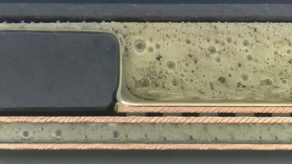
Microsection analysis of an embedded component PCB cavity showing resin voids and trapped gas bubbles in the dielectric layer.
The five most important failure families are delamination, microvia failure, component damage, void-related defects and registration errors. Each must be connected to a measurable manufacturing variable so that the supplier can prevent recurrence rather than only inspect the final board.
| Failure mode | Typical physical cause | Manufacturing control | Verification |
| Delamination | Poor resin wetting, trapped gas, excessive stress, contamination | Surface prep, vacuum lamination, resin-flow review, press-profile control | Cross-section, visual inspection, thermal/mechanical testing |
| Microvia failure | Weak Cu interface, voids, poor desmear, aggressive geometry | Laser energy control, desmear, seed/copper control, fill verification | Via-chain electrical test, cross-section, thermal cycling |
| Component cracking | Excessive mechanical or thermal stress | Cavity clearance, component handling, press-force/profile control | X-ray/CT where applicable, cross-section, electrical test |
| Voids | Incomplete resin flow or trapped gas | Vacuum lamination, resin system selection, cavity/feature design | Cross-section, X-ray/CT for suitable constructions |
| Registration failure | Layer movement, cavity drift, drill/laser offset | Tooling targets, optical registration, statistical process control | AOI, X-ray, cross-section, dimensional inspection |
How is cavity geometry controlled for embedded‑component PCB manufacturing?
Cavity geometry should be treated as a controlled mechanical feature, not merely as an opening in the PCB. The drawing should define cavity length/width, depth, corner condition, component clearance, reference datums and allowable registration error.
Practical engineering control example:
- Define the finished component envelope first, then calculate cavity clearance from the actual component tolerance—not nominal CAD dimensions alone.
- For a 2.0 mm component-to-cavity wall gap used in a specific reliability test vehicle, the gap itself was a controlled experimental variable; it should not be copied as a universal design rule.
- For deep cavities, monitor depth at multiple locations because bottom-plane nonuniformity can change resin flow and local stress.
- Use optical/X-ray registration data to correlate cavity position, component position and subsequent laser-via position.
Manufacturing pain point: A cavity can be dimensionally acceptable while the embedded component is still electrically marginal if the subsequent laser via lands too close to the component terminal or target pad edge. The real control chain is cavity → component → dielectric thickness → laser via → copper fill → final electrical continuity.
How do laser drilling and mSAP processes impact embedded PCB reliability?
Advanced HDI manufacturing increasingly uses tightly controlled CO₂ or UV laser drilling and mSAP/SAP-compatible copper structures to support finer interconnects. These processes improve density, but they also reduce the process margin available for drilling, registration, plating and copper-interface defects.
Key parameters to control include:
- Laser spot/beam condition and energy window
- Copper thickness before laser drilling
- Dielectric thickness above the target
- Via opening and capture-pad dimensions
- Desmear and hole-wall preparation
- Electroless copper initiation
- Electrolytic copper thickness and fill behavior
- Pattern-plate etch compensation and final trace geometry
Why this matters : Current industry equipment and chemistry developments are explicitly targeting next-generation HDI, mSAP and advanced packaging, including low-etch-depth laser-drill pretreatment, more uniform copper deposition, blind-microvia filling and digital process control. These developments are particularly relevant where an embedded component is connected through fine-pitch HDI structures.
What are the most difficult manufacturing problems with embedded component PCBs?
The hardest problems are process interactions: resin flow around a non-standard component, registration through multiple process cycles, hidden interfaces that cannot be fully inspected from the surface, and microvia reliability after thermal exposure.
Detailed manufacturing pain points:
- Resin starvation or resin-rich regions around the component can create local mechanical and dielectric variation.
- Component thickness variation changes the final embedded dielectric thickness and therefore changes via depth and impedance geometry.
- A component can move during lamination, making the later laser-via target effectively shift even when the laser machine itself is stable.
- Multiple press cycles can accumulate registration error. A design that is safe after one build-up cycle may lose margin after several sequential lamination steps.
- Lead-free reflow adds a severe thermal preconditioning event before field operation; marginal microvia interfaces can become latent failures.
- Fine-line/mSAP structures reduce copper thickness and etch margin, so contamination, over-etch or under-etch can have a larger percentage impact on the finished conductor.
- Traditional visual inspection cannot prove the internal quality of every embedded interface; destructive cross-section and electrical reliability coupons remain important.
How does thermal cycling affect an embedded component PCB?
Thermal cycling accelerates defects that depend on CTE mismatch, copper fatigue, interface adhesion, microvia construction and lamination quality. The correct temperature range and cycle count must be defined by the application and qualification plan rather than selected arbitrarily.
A parameterized qualification plan can specify:
- Low-temperature limit: T_low = application-specific requirement
- High-temperature limit: T_high = application-specific requirement
- Ramp rate: controlled and recorded
- Dwell: defined at each temperature extreme
- Cycle count: N cycles selected from the product risk profile
- Electrical criterion: continuity/resistance threshold defined before testing
- Post-test inspection: cross-section plus failure analysis if electrical drift occurs
Verified industry reference point: IPC technical work has reported microvia thermal-cycling experiments using 150°C, 170°C and 180°C test conditions for 1,000 cycles, while another qualification study used −55°C to +125°C cycling and approximately 15-minute dwells at each extreme. These are test-program examples, not automatic acceptance limits for every embedded PCB.
How should microvia reliability be validated for embedded component PCBs?
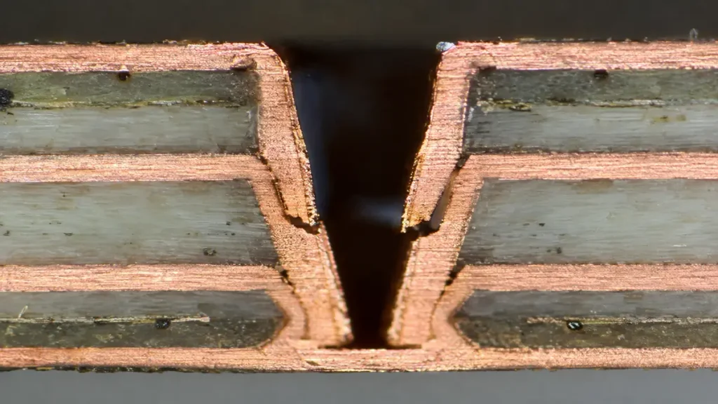
High-magnification microsection analysis of a laser-drilled microvia showing plating cracks and interface separation under stress.
Microvia reliability should be validated with both structural evidence and performance-based electrical testing, especially when stacked or sequentially built microvias connect to embedded components.
A robust validation matrix can include:
- Via-chain resistance monitoring during thermal cycling
- Cross-section of representative production coupons
- Micro-etch evaluation of copper interfaces
- Copper-fill/void inspection
- Preconditioning that reproduces the intended lead-free assembly exposure
- Thermal shock or thermal cycling appropriate to the product
- Electrical insulation/continuity testing
- Failure localization and metallographic analysis
Engineering warning: IPC has documented latent microvia failures that may not appear during room-temperature inspection and has emphasized performance-based testing because traditional microsection inspection alone may not expose every weak interface. For stacked microvias, the Cu/Cu junction is a critical reliability location.
What does a production-ready embedded component PCB reliability control plan look like?
A production-ready plan links every critical feature to a measurable input, an inspection method, a sampling strategy and a reaction rule.
| Process | Critical parameter | Example control target | Evidence | Reaction |
| Incoming component | Thickness / terminal geometry | Use actual supplier tolerance; lock revision | COC + dimensional record | Hold and engineering review |
| Cavity formation | X/Y/depth/registration | Drawing-defined tolerance | AOI/optical measurement | Rework/stop if out of limit |
| Placement | X/Y/theta | Placement tolerance tied to via keep-out | Optical/X-ray as applicable | Adjust placement program |
| Lamination | Pressure/time/temp/vacuum | Validated press recipe | Press data log | Recipe correction + lot review |
| Laser via | Opening/target alignment | Drawing-defined via/pad geometry | Laser SPC + coupon cross-section | Hold lot if trend breaches limit |
| Copper plating | Thickness/fill/interface | Customer/IPC requirement + process window | Thickness map + cross-section | Bath/process correction |
| Final test | Continuity/insulation | Released electrical criteria | E-test + reliability data | Failure analysis |
Why is prototype reliability validation critical before volume production?
Prototype reliability testing converts hidden manufacturing assumptions into measurable evidence before tooling, material and assembly costs scale up.
For an embedded component PCB, prototype validation should deliberately challenge:
- The worst-case component thickness and cavity clearance
- The longest registration chain in the stack-up
- The most thermally stressed microvia structure
- The most difficult resin-flow region
- The highest-density BGA/HDI connection zone
- The final assembly reflow profile expected by the customer
Recommended engineering sequence: prototype → cross-section baseline → electrical baseline → thermal/mechanical preconditioning → post-test electrical check → failure analysis if needed → design/process correction → repeat build → pilot lot → volume release.
How can embedded component PCB reliability be improved at the design stage?
The most effective reliability improvement is to remove avoidable process sensitivity before fabrication begins.
- Select components whose thickness, termination and thermal limits are compatible with the PCB process.
- Keep cavity geometry compatible with routing, lamination and laser-drill registration.
- Choose dielectric thickness with both impedance and microvia aspect-ratio requirements in mind.
- Avoid unnecessarily aggressive stacked-via geometry when a staggered or simpler structure meets the electrical requirement.
- Define test coupons that reproduce the actual embedded interconnect—not a generic through-hole coupon.
- Specify the reliability test matrix in the RFQ or fabrication drawing so suppliers quote the same technical requirement.
- Require lot-level traceability for material, lamination recipe, plating process and reliability coupon results.
What should PCB buyers ask an embedded component PCB supplier ?
Buyers should evaluate process capability and reliability evidence—not simply the supplier’s stated minimum line/space or minimum via size.
- Can you provide a cross-section of the actual embedded component construction, including cavity, dielectric, component terminal and laser-via interfaces?
- What is your controlled process window for cavity registration, lamination and laser-via targeting?
- How do you validate stacked or embedded microvia reliability after lead-free thermal preconditioning?
- Which parameters are recorded for each production lot, and which records can be included in the FA/PPAP or FAI package?
- Can you build a pilot coupon that reproduces the highest-risk component, cavity and HDI interconnect rather than using a generic reliability coupon?
What are the five Google-search FAQs procurement teams ask about embedded component PCB suppliers?
What are the five Google-search FAQs procurement teams ask about embedded component PCB suppliers?
Look for demonstrated cavity machining, controlled lamination, laser microvia formation, copper filling, cross-section capability and reliability testing. Ask for process evidence tied to your actual stack-up rather than a generic capability chart.
Can a PCB supplier manufacture embedded component HDI PCBs with fine-pitch BGA connections?
Yes, but the supplier must control component-to-cavity registration, dielectric thickness, laser-via targeting, copper fill and sequential lamination as one integrated process. Ask for a cross-section of the proposed structure before releasing volume tooling.
How do I verify embedded component PCB reliability before mass production?
Use a pilot build with production-intent materials and processes, establish baseline electrical measurements, then run application-specific thermal/mechanical testing and post-test cross-sections. Reliability should be demonstrated on the actual risk structure.
What PCB reliability documents should a supplier provide during qualification?
A practical package can include material certificates, stack-up, dimensional inspection, cross-sections, microvia evaluation, electrical test results, thermal-cycle records, failure-analysis reports and lot traceability. The exact package should be agreed in the purchase specification.
How can I reduce embedded component PCB manufacturing risk and cost?
Reduce risk before tooling by freezing component tolerances, cavity dimensions, dielectric thickness, via geometry and test criteria during the RFQ/DFM stage. A slightly less aggressive stack-up that has a larger process window can be cheaper overall than a nominally lower-cost design with repeated yield failures.
What is the final reliability principle for embedded component PCBs?
The embedded component must be qualified as part of the PCB structure. Component selection, cavity design, stack-up, materials, lamination, laser drilling, copper deposition, microvia architecture and reliability testing form one engineering chain.
At Shenzhen Hongda Circuit Technology Co., Ltd., the practical manufacturing objective is to convert that chain into measurable controls: define the critical dimensions, identify the highest-risk interfaces, build production-intent coupons, record process data, verify the hidden interconnects and use failure analysis to close the loop. That approach is more meaningful to a procurement engineer than a simple ‘minimum via’ or ‘minimum line/space’ claim because reliability depends on the complete construction.
Technical references used for verification
- IPC-7092, Design and Assembly Process Implementation for Embedded Components.
- IPC-6012F, Qualification and Performance Specification for Rigid Printed Boards.
- IPC-TM-650 Test Methods Manual, including thermal shock/thermal cycling methods.
- IPC technical work on microvia reliability and performance-based acceptance testing.
- Industry manufacturing developments covering advanced HDI, mSAP, laser drilling, blind-microvia filling and digital process control.
Shenzhen Hongda Circuit Technology Co., Ltd. | pcb@pcbkr.com | www.pcbkr.com
About Author
David Chen https://www.linkedin.com/in/pcbcoming
David Chen boasts an extensive professional background in PCBA manufacturing, PCBA testing, and PCBA optimization, with specialized expertise in high-precision PCBA fault analysis and rigorous PCBA reliability testing. The author has worked with high-layer-count server PCB fabrication, ultra-low-loss backplane stackups, and thermo-mechanical reliability optimization for AI infrastructure projects involving 112G and 224G PAM4 architectures. Skilled in complex circuit design and cutting-edge advanced PCB manufacturing processes, he delivers solutions that elevate product durability and performance across industrial applications. His technical articles focusing on PCBA manufacturing workflows and testing methodologies are widely cited by industry peers, research institutions, and technical platforms, solidifying his reputation as a recognized technical authority in the global circuit board manufacturing sector.