Multilayer PCB Manufacturing Cost in 2026: Tech & Design Optimization
How Shenzhen Hongda Circuit Technology Delivers a Competitive Edge.
As AI infrastructure, high-speed computing, and next-generation electronics continue to reshape the global electronics supply chain, multilayer PCB manufacturing cost has become one of the most scrutinized variables in B2B procurement. The decisions made at the design stage — long before a Gerber file is submitted — determine whether a project lands on budget or spirals into expensive engineering revisions.
This article draws on Shenzhen Hongda Circuit Technology Co., Ltd.’s operational experience and the most significant PCB manufacturing technology advancements entering commercial production in 2026. It is written for engineers, procurement managers, and product teams who need grounded technical insight alongside practical cost guidance.
Why Multilayer PCB Manufacturing Cost Is a Strategic Concern in 2026
The cost of a multilayer printed circuit board is no longer simply a line item in a bill of materials. For AI accelerator boards, GPU compute cards, data center backplanes, and advanced automotive electronics, PCB cost directly influences total system economics, time-to-market, and manufacturing yield at scale.
Several factors have intensified cost pressure entering 2026:
- Layer counts in high-performance applications now routinely reach 20 to 40 layers, with some AI inference boards exceeding 50 layers.
- High-speed material requirements — including PTFE-based laminates, hydrocarbon ceramics, and low-loss prepregs — have experienced continued supply volatility.
- Geopolitical sourcing shifts have altered raw material costs for copper foil and specialty laminates used in advanced PCB fabrication.
- Tighter signal integrity requirements (PCIe Gen 5/6, 112G SerDes, NVLink) mandate fabrication processes that directly increase per-unit cost.
Understanding where cost originates — and how design choices amplify or reduce that cost — is the foundation of every successful procurement strategy.
Key Cost Drivers in Multilayer PCB Fabrication: A Technical Breakdown
Cost in multilayer PCB manufacturing is not linear. It compounds at multiple process stages. The following drivers represent the most significant contributors across the fabrication workflow.
Layer Count and Lamination Cycles
Each lamination cycle in multilayer PCB construction adds process time, material cost, and yield risk. A 4-layer board completes a single press cycle; a 20-layer board may require four or more sequential laminations. Each cycle introduces thermal stress, dimensional variation, and the potential for delamination at inner layer interfaces.
For HDI designs requiring sequential build-up (SBU) processes, the number of lamination cycles can become the single largest cost variable, particularly when combined with laser-drilled microvias at each stage.
Material Selection: FR-4, High-Speed Laminates, and the 2026 Material Landscape
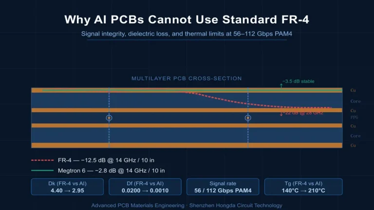
Standard FR-4 remains the default for cost-sensitive designs below 5 GHz. However, signals operating above 10 GHz — including PCIe Gen 5, 400G Ethernet, and millimeter-wave radar — require laminates with controlled dielectric constant (Dk) and dissipation factor (Df).
In 2026, three material tiers dominate advanced multilayer PCB fabrication:
- Modified FR-4 / High-Tg FR-4: Suited for standard multilayer designs up to 8 to 12 GHz with modest signal integrity requirements.
- Megtron 6 / Rogers 4350B class laminates: Preferred for server backplanes, AI compute cards, and high-speed networking boards requiring consistent Dk across temperature ranges.
- PTFE-based and ceramic-filled composites: Required for mmWave applications (automotive radar, 5G base stations, satellite communication) where Df below 0.003 is non-negotiable.
Material cost premiums for high-speed laminates can range from 3x to 8x compared to standard FR-4, making material selection one of the most impactful early-stage design decisions.
Via Structures: Through-Hole, Blind, Buried, and Microvia Cost Implications
Via technology is a primary cost lever in multilayer PCB manufacturing. Through-hole vias remain the lowest-cost option, compatible with standard drilling and plating processes. Blind vias (connecting the surface to an inner layer) and buried vias (connecting inner layers without reaching the surface) require additional lamination and drilling cycles, significantly increasing fabrication complexity.
Laser-drilled microvias — standard in HDI PCB manufacturing — introduce further cost through:
- CO2 or UV laser drilling equipment with tighter positional tolerances than mechanical drilling.
- Additional plasma desmear and copper plating steps for each microvia layer.
- Higher alignment precision requirements between sequential build-up layers.
The cost premium for HDI structures versus standard multilayer boards typically ranges from 40% to 120% depending on via density, layer count, and whether via-in-pad processes are required.
Copper Thickness, Heavy Copper PCB Fabrication, and Current Capacity Trade-offs
Standard PCB fabrication uses 0.5 oz to 2 oz copper (17 to 70 microns). Heavy copper PCB manufacturing — defined by copper weights of 3 oz and above — introduces fabrication challenges that directly translate to higher cost:
- Etching control becomes more demanding as thicker copper requires longer exposure to etchant, increasing the risk of undercutting fine traces.
- Plating uniformity across high-aspect-ratio holes and thick copper layers requires tighter bath chemistry control.
- Fine-line resolution decreases with copper weight, limiting routing density.
- Thermal management during lamination must account for differential expansion coefficients across thick copper and dielectric layers.
Heavy copper PCBs are essential for power electronics, EV battery management systems, and industrial motor drives — but engineers should specify copper weight based on verified current and thermal models rather than assumed design margins.
2026 PCB Manufacturing Technology Advances That Are Reshaping Cost and Performance
The PCB fabrication industry entered 2026 with several manufacturing technology advances moving from early adoption into broader commercial availability. These developments create new cost-performance trade-offs that procurement teams and design engineers must understand.
Advanced Backdrilling Technology for High-Speed Signal Integrity
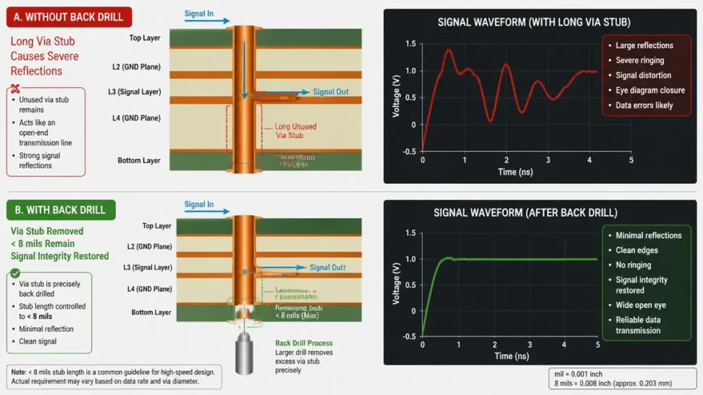
Backdrilling — also known as controlled-depth drilling or via stub removal — has become standard practice for high-speed PCB designs operating above 10 Gbps. Via stubs act as transmission line discontinuities, creating signal reflections that degrade channel performance at high data rates.
In 2026, backdrilling technology has advanced in two significant directions:
- Precision depth control: CNC backdrilling machines now achieve stub lengths below 8 mils (200 microns) with tighter process capability than 2023 equipment, reducing signal integrity variation across production panels.To better grasp the electrical impact of via stubs, the technical simulation below contrasts a non-backdrilled channel against an optimized structure with a stub under 8 mils:
- Selective backdrilling automation: Advanced CAM software enables automatic identification of high-speed nets requiring backdrilling, reducing engineering time and programming errors.
Despite these improvements, backdrilling adds cost through additional CNC programming, specialized tooling, increased drilling time, and mandatory post-drill inspection. The decision to backdrill should be driven by channel simulation data — applying backdrilling indiscriminately increases cost without commensurate signal integrity benefit.
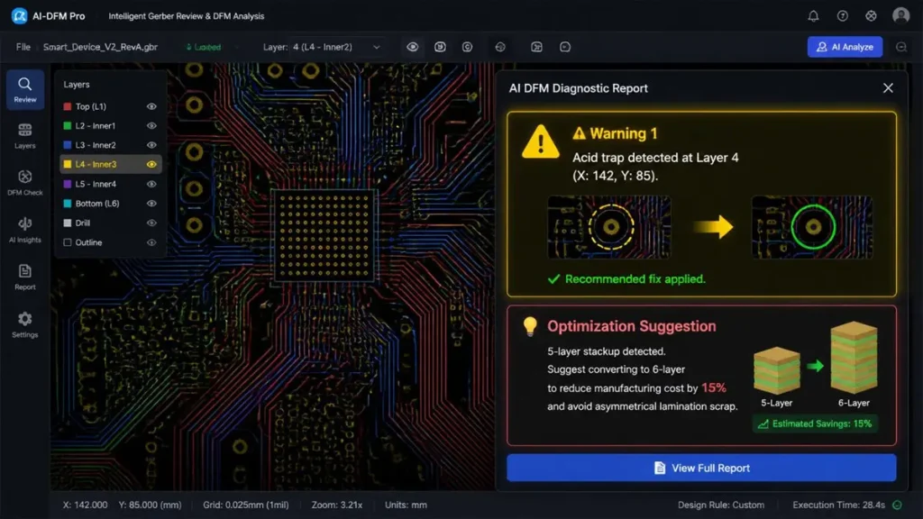
AI-Assisted Design for Manufacturability (DFM) in PCB Fabrication
Advanced Multilayer PCB Sourcing Benchmarks (112G PAM4, High Layer Counts, and Precision Mechanical & Laser Drilling Limits)
One of the most practically impactful developments entering 2026 commercial production is AI-assisted DFM analysis integrated directly into the fabrication quoting and engineering review workflow. Leading PCB manufacturers — including Shenzhen Hongda Circuit Technology Co., Ltd. — have implemented machine learning-based DFM tools that:
- Identify yield risk factors in Gerber files before production begins, catching issues such as acid traps, insufficient annular rings, and copper-to-edge clearance violations.
- Recommend stackup modifications that reduce lamination cycles while maintaining impedance targets.
- Flag unnecessary HDI structures where standard through-hole vias would satisfy routing requirements.
- Estimate the yield impact of specific design choices, enabling designers to make informed cost-versus-performance trade-offs before tooling is committed.
Early DFM collaboration — submitting preliminary Gerber files for AI-assisted review before final design freeze — is now one of the highest-ROI activities available to engineering teams targeting cost reduction without compromising electrical performance.
Embedded Component PCB Technology and Integration Cost
Embedded passive and active component integration — placing resistors, capacitors, and in some cases ICs within the PCB substrate rather than on its surface — has matured significantly by 2026. This technology delivers system-level benefits including reduced board real estate, improved parasitic performance for decoupling capacitors, and lower assembly component count.
However, embedded component PCB fabrication introduces cost considerations that require careful evaluation:
- Component-in-laminate processes require specialized cavity machining and precise component placement within the PCB stack, adding fabrication steps.
- Rework options for embedded components are extremely limited, making yield management during fabrication critical.
- The technology is best justified for high-volume applications where assembly cost savings and board size reduction offset the higher bare board cost.
For most B2B applications in 2026, embedded components remain most economical at volumes above 10,000 units per year, where per-unit savings on SMT assembly and improved electrical performance justify the fabrication premium.
Glass Substrate and Ultra-Thin Dielectric Technologies for AI Chiplet Packaging
At the leading edge of PCB and substrate technology in 2026, glass core substrates and panel-level fan-out packaging are emerging as alternatives to traditional organic laminates for AI chiplet interconnect and advanced packaging applications. While not conventional PCB territory, these technologies influence the high-end multilayer substrate market:
- Glass substrates offer near-zero coefficient of thermal expansion (CTE), superior dimensional stability for fine-pitch interconnect, and higher thermal conductivity compared to organic laminates.
- Ultra-thin dielectrics (below 25 microns per layer) enable routing density approaching silicon interposer performance at significantly lower cost than 2.5D silicon packaging.
- Panel-level glass processing remains in early commercialization in 2026, with volume production yields still maturing — making cost per unit higher than established HDI organic processes for the near term.
For design teams working on next-generation AI compute platforms, understanding where glass substrate technology sits in the cost-performance landscape is essential for roadmap planning, even if current production remains on organic HDI platforms.
Design Choices That Increase Multilayer PCB Manufacturing Cost — and How to Avoid Them
The most preventable source of excess PCB cost is design decisions made without manufacturing awareness. The following patterns consistently generate unnecessary cost in multilayer PCB fabrication.
Odd-Layer Stackups and Panelization Inefficiency
Multilayer PCBs are constructed in even-layer pairs for symmetrical lamination. A 5-layer design requires a 6-layer lamination process; a 7-layer design requires an 8-layer process. Odd-layer stackups do not reduce fabrication cost — they increase it by creating asymmetric stress and requiring additional balancing layers or process compensations.
The practical guidance is straightforward: always use even-numbered layer counts. A 6-layer design costs less than a 5-layer design attempting to achieve the same routing in fewer layers with non-standard process steps.
Over-Specification of HDI Blind and Buried Via Structures
HDI via structures — blind vias, buried vias, and stacked microvias — are engineered solutions for routing-density-constrained designs. They are not default via options. Each sequential lamination cycle required by HDI structures adds process cost, reduces yield, and extends fabrication lead time.
Before specifying blind or buried vias, design teams should evaluate:
- Whether increased layer count in a standard through-hole via design would provide adequate routing clearance at lower total cost.
- Whether component placement optimization could reduce the routing density that drives HDI requirements.
- Whether the application genuinely requires HDI density (mobile/wearable with extreme space constraints) or whether HDI was inherited from a reference design without verification.
Excessive Copper Weight Specification Without Load Analysis
Heavy copper PCB manufacturing is specified for applications requiring high continuous current, such as power bus bars, EV charging controllers, and industrial power converters. However, copper weight is often over-specified based on design habit rather than verified current density analysis.
Every increase in copper weight above standard 1 oz (35 microns) increases both raw material cost and process complexity. Specifying 3 oz copper on a board where 2 oz would satisfy verified thermal and current requirements adds cost with no functional benefit. Thermal simulation-based copper weight specification is a recommended practice for any design exceeding standard current levels.
Cost vs. Signal Integrity: Engineering the Right Balance for High-Speed PCB Designs
High-speed PCB designs create genuine tension between signal integrity requirements and manufacturing cost. The goal is not to minimize cost at the expense of performance, but to spend fabrication budget precisely where signal integrity demands it.
When Backdrilling Is Non-Negotiable in High-Speed PCB Manufacturing
Backdrilling becomes non-negotiable at data rates above 10 Gbps on boards with more than 8 layers, where via stub resonance falls within the operating frequency band. Specific applications where backdrilling is consistently required include:
- PCIe Gen 4, Gen 5, and Gen 6 slot interconnects on server motherboards and AI compute platforms.
- 112G PAM4 and 224G PAM4 SerDes lanes on switching ASICs and high-speed networking equipment.
- High-speed memory interfaces (HBM3, GDDR7) on AI accelerator PCBs.
- NVLink and other proprietary GPU interconnects requiring consistent channel loss below defined masks.
For these applications, backdrilling cost is not optional — it is a fabrication requirement for meeting signal integrity specifications. The question is not whether to backdrill, but how to minimize backdrilling cost through selective application to only the high-speed nets that require it.
Material Selection Trade-offs: When High-Speed Laminates Justify Their Premium
High-speed laminates are justified when trace insertion loss, skew, and impedance stability across temperature and frequency are critical to application performance. They are frequently over-specified when:
- Signal frequencies are below 6 GHz and standard high-Tg FR-4 provides adequate Dk stability.
- Loss budget analysis shows standard materials meet channel requirements with modest trace length adjustments.
- The design uses high-speed materials on layers where signal frequencies are actually low (power planes, low-speed control signals).
A targeted approach — using high-speed laminate only in the specific layers carrying the critical high-frequency signals, with standard FR-4 on remaining layers — is a hybrid strategy that reduces material cost while maintaining the signal integrity performance where it is genuinely needed.
Practical Multilayer PCB Cost Optimization Strategies for 2026 Projects
The following strategies represent proven approaches to reducing multilayer PCB manufacturing cost without compromising the electrical and mechanical performance requirements of the application.
- Use even-numbered layer stackups in all designs. The fabrication cost of a 5-layer board exceeds that of a properly designed 6-layer board in most production scenarios.
- Conduct via technology review before design freeze. Quantify the routing density benefit of each HDI via type against its fabrication cost premium. Default to through-hole vias where routing allows.
- Perform current density and thermal analysis before specifying copper weight. Simulation-based copper specification eliminates unnecessary heavy copper processing costs.
- Apply selective backdrilling based on channel simulation data. Identify high-speed nets requiring stub removal and limit backdrilling to those nets rather than applying it board-wide.
- Standardize laminate materials across product families. Non-standard materials generate minimum order quantities, longer lead times, and procurement complexity that compound per-unit cost.
- Submit Gerber files for DFM review before final design freeze. Catching manufacturability issues at the design stage eliminates costly engineering revision cycles after tooling has been committed.
- Share target application context with your PCB manufacturer. Providing application details — AI server, GPU board, automotive radar, industrial power converter — enables the manufacturer to suggest process optimizations relevant to the actual operating environment.
- Evaluate panelization efficiency during layout. Board outline, tooling strip requirements, and panel utilization rate directly influence per-unit fabrication cost in production volumes.
How Shenzhen Hongda Circuit Technology Co., Ltd. Supports Cost-Optimized Multilayer PCB Manufacturing
Shenzhen Hongda Circuit Technology Co., Ltd. operates as a full-service multilayer PCB manufacturer serving B2B clients across AI infrastructure, high-speed networking, industrial electronics, automotive, and power electronics sectors. The company’s engineering approach emphasizes early collaboration as the primary mechanism for delivering competitive multilayer PCB manufacturing cost without sacrificing fabrication quality.
DFM-First Quoting and Engineering Collaboration
Hongda’s quoting process integrates DFM analysis from the first submission. Design teams are encouraged to provide:
- Complete stackup definitions including dielectric materials, copper weights per layer, and impedance targets.
- Via technology breakdown distinguishing through-hole, blind, buried, and microvia structures.
- Target application description to enable process-specific optimization recommendations.
- Volume scaling targets for panelization and tooling cost amortization planning.
This upfront information enables Hongda’s engineering team to identify cost reduction opportunities during the quoting stage — before tooling costs are incurred and design changes are expensive.
Impedance Control, Backdrilling Precision, and High-Speed PCB Fabrication Capabilities
Shenzhen Hongda Circuit Technology Co., Ltd. maintains production capabilities across the multilayer PCB technology spectrum, including:
- Controlled impedance fabrication with coupon-based TDR verification across production panels.
- Backdrilling with stub length control to customer-specified tolerances for high-speed channel compliance.
- HDI sequential lamination for blind and buried via designs serving mobile, wearable, and high-density compute applications.
- Heavy copper PCB fabrication for power electronics applications requiring 3 oz to 10 oz copper per layer.
- High-speed laminate processing including Megtron 6, Rogers series, and PTFE-based materials for mmWave and high-frequency applications.
Getting a Competitive PCB Quote: What to Prepare
To receive the most accurate and cost-optimized multilayer PCB manufacturing quote from Shenzhen Hongda Circuit Technology Co., Ltd., design teams should prepare the following:
- Gerber files including all copper layers, solder mask, silkscreen, drill files, and board outline.
- Complete stackup specification with dielectric material callouts and impedance requirements.
- Layer count, board dimensions, and minimum feature size (trace width, space, drill diameter).
- Surface finish specification (ENIG, HASL, OSP, hard gold) and any special process requirements.
- Target quantity and expected production volume scaling for panelization optimization.
- Application context and any specific quality or testing requirements (IPC Class 2 vs. Class 3, AOI, X-ray, electrical test).
Early submission of even preliminary Gerber files enables DFM feedback that consistently reduces final production cost compared to designs submitted cold at the tooling stage.
Conclusion: Multilayer PCB Manufacturing Cost Is an Engineering Outcome, Not Just a Vendor Variable
The data consistently shows that multilayer PCB manufacturing cost is determined more by design decisions than by fabrication pricing. Layer count, via technology selection, material specification, copper weight, and the decision of when to apply backdrilling each carry significant cost implications that are established at the design stage — not the procurement stage.
As PCB manufacturing technology continues to advance through 2026 and beyond — with AI-assisted DFM, precision backdrilling, embedded component integration, and glass substrate technologies reshaping the cost-performance frontier — the manufacturers who deliver sustained value are those who combine technical fabrication capability with genuine engineering partnership.
Shenzhen Hongda Circuit Technology Co., Ltd. is committed to that partnership approach: providing transparent DFM feedback, process-specific optimization guidance, and multilayer PCB fabrication capabilities that serve the full spectrum of modern high-speed and high-reliability applications.
For inquiries, DFM review requests, or multilayer PCB manufacturing quotations, contact Shenzhen Hongda Circuit Technology Co., Ltd. directly with your design files and application requirements.© 2026 Shenzhen Hongda Circuit Technology Co., Ltd. All rights reserved. This article is intended for informational purposes for engineering and procurement professiona
FAQ
Why is odd-layer stackup design actively discouraged in high-reliability multilayer PCB manufacturing?
Multilayer PCBs are constructed in symmetrical even-layer pairs to ensure dimensional stability and uniform distribution of heat and stress during lamination cycles. Designing an odd-layer board (e.g., 5 or 7 layers) does not save money; instead, it forces the factory to use asymmetric process adjustments or add useless balancing copper layers to prevent board warping. This significantly reduces panel utilization and increases scrap risk.
At Shenzhen Hongda Circuit, our engineering team routinely recommends converting odd-layer designs to standard even-layer configurations (like moving from 5 to 6 layers) during DFM reviews, which simplifies fabrication and immediately drops your per-unit costs.
How do high-speed laminates like Megtron 6 or Rogers impact the overall multilayer PCB manufacturing cost?
Sourcing premium low-loss or ultra-low-loss laminates introduces a massive raw material premium, often driving the cost 3x to 8x higher than standard high-Tg FR-4. These materials are essential for AI servers or high-frequency mmWave radar modules operating above 10 GHz to control dielectric constant (Dk) and dissipation factor (Df) variations.
To optimize your budget without failing signal integrity specifications, you can implement a hybrid stackup strategy. This means using high-speed laminates exclusively on the specific layers carrying critical high-frequency signals (like PCIe Gen 5/6 or 112G SerDes lines) while utilizing standard FR-4 for power and ground planes to significantly reduce material costs.
When is backdrilling genuinely necessary for high-speed digital PCBs, and how can we minimize its processing cost?
Backdrilling (controlled-depth drilling) becomes technically non-negotiable at data rates above 10 Gbps on boards exceeding 8 layers. In applications like AI accelerator platforms (using HBM3 or GDDR7) and PCIe slot interconnects, via stubs act as transmission line discontinuities that ruin signal integrity. Backdrilling removes these stubs to stop signal reflections.
However, applying backdrilling board-wide adds substantial costs due to additional CNC programming, specialized tooling, and mandatory post-drill inspections. The smartest cost-optimization strategy is to apply backdrilling selectively—only targeting critical high-speed differential nets based on your pre-layout channel simulation data rather than processing the entire panel.
Why should I avoid specifying excessive copper weights, and how does heavy copper affect PCB fabrication costs?
While heavy copper PCB manufacturing (3 oz to 10 oz per layer) is crucial for carrying high continuous currents in power electronics and EV battery management systems, over-specifying copper thickness creates severe manufacturing complexity that directly inflates costs. Heavy copper requires longer chemical etching times, which increases the risk of undercutting fine traces and severely reduces your routing density. It also demands tighter control over plating uniformity across high-aspect-ratio holes and complicates thermal management during lamination.
Engineers should always perform precise current density and thermal simulations to specify copper weights based on real load demands rather than arbitrary safety margins.
What information must be submitted to a PCB manufacturer upfront to secure the most competitive and accurate quote?
To get a highly optimized, production-ready quote from an advanced manufacturer like Shenzhen Hongda Circuit, you should move past submitting generic catalog claims or incomplete archives. Providing a 1. 1. comprehensive engineering dataset from day one allows the factory to maximize panelization efficiency and apply AI-assisted DFM tools to spot yield risks before tooling is committed.
Your quotation package should include:
1. Complete Gerber or ODB++ files including all copper layers, drill files, and the exact board outline.
2. A fully defined stackup specification with detailed dielectric material callouts, impedance control targets, and copper weights per layer.
3. A clear via technology breakdown (distinguishing standard through-holes from HDI blind, buried, or stacked microvias).
4.The target application context (e.g., AI server, GPU compute card, automotive radar) which enables our engineers to suggest process-specific cost reductions relevant to your operating environment.
About Author
David Chen https://www.linkedin.com/in/pcbcoming
David Chen boasts an extensive professional background in PCBA manufacturing, PCBA testing, and PCBA optimization, with specialized expertise in high-precision PCBA fault analysis and rigorous PCBA reliability testing. The author has worked with high-layer-count server PCB fabrication, ultra-low-loss backplane stackups, and thermo-mechanical reliability optimization for AI infrastructure projects involving 112G and 224G PAM4 architectures. Skilled in complex circuit design and cutting-edge advanced PCB manufacturing processes, he delivers solutions that elevate product durability and performance across industrial applications. His technical articles focusing on PCBA manufacturing workflows and testing methodologies are widely cited by industry peers, research institutions, and technical platforms, solidifying his reputation as a recognized technical authority in the global circuit board manufacturing sector.