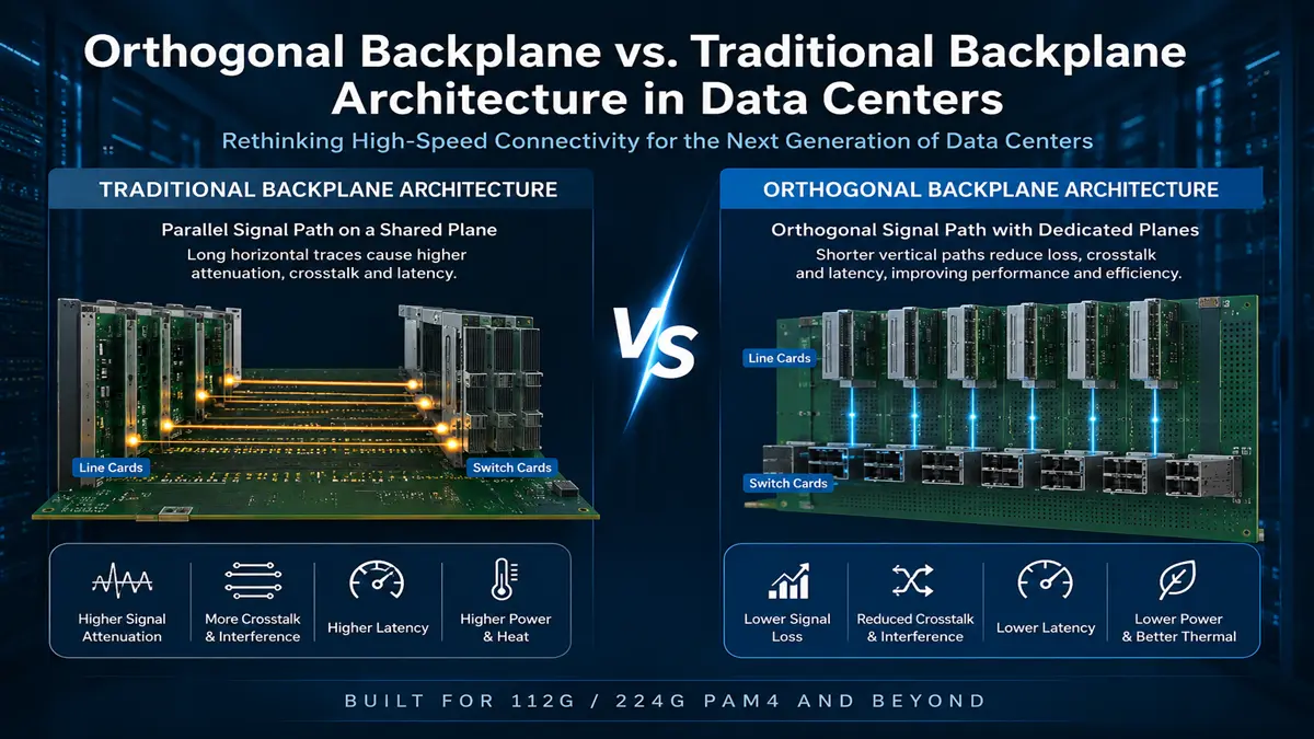
What is the difference between an orthogonal backplane and a traditional backplane architecture in data centers?
In the hardware development of next-generation data center clusters, optimizing copper interconnect topologies to mitigate extreme high-speed signal attenuation has become a critical challenge shared by system architects and procurement decision-makers. With the broad adoption of 112G PAM4 signaling and the sequential transition toward 224G PAM4 architectures, deploying a high-performance Orthogonal Backplane PCB design is demonstrating superior electrical and thermal performance over traditional parallel-plane frameworks in specific ultra-high-density, high-bandwidth hardware use cases.
1. Understanding Backplane Evolution: Traditional vs. Orthogonal Frameworks
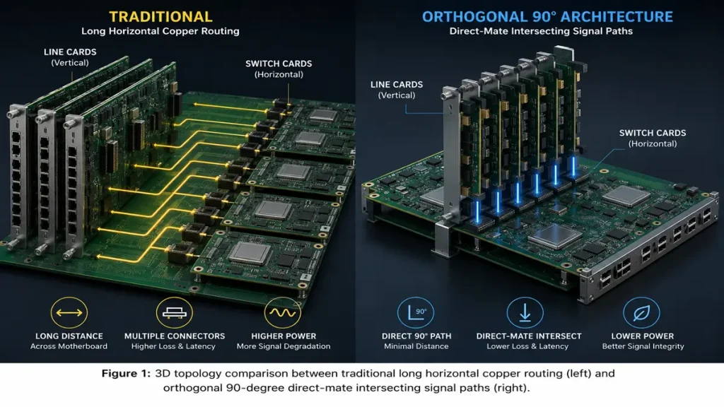
3D topology comparison between traditional long horizontal copper routing (left) and orthogonal 90-degree direct-mate intersecting signal paths (right).
The Legacy Model: Traditional Backplane Architecture
Traditional backplane design relies on a large, passive copper motherboard (the main backplane) mounted at the rear of the system chassis. In this topology, all line cards and fabric/switch cards are plugged into this single motherboard plane in a parallel vertical or horizontal arrangement.
Signals traveling from a front-facing line card must pass through a card-edge connector, traverse long horizontal copper traces across the backplane motherboard (often ranging from 15 to 20 inches, or 380 mm to 500 mm Industry Experience Value), and enter the switch card via a secondary connector. At frequencies required for 56G PAM4 (28 GHz) or 112G/224G PAM4 (56 GHz Nyquist), these long copper paths introduce severe skin effect and dielectric losses, which can cause significant eye diagram closure and drive bit error rates (BER) beyond acceptable boundaries under specific signaling conditions.
The Structural Shift: Orthogonal Backplane PCB Architecture
An orthogonal architecture alters the spatial geometry of the system to shorten signal pathways. It rotates the fabric/switch cards by 90 degrees relative to the line cards (for example, utilizing vertical line cards in the front and horizontal switch cards in the rear).
By positioning these slots at a precise right angle, the signal paths of the front and rear cards intersect directly at their crossover points. In mass production, this spatial alignment is primarily implemented in two forms:
- Orthogonal Midplane: Cards interface via a relatively thin midplane, where internal routing is limited to ultra-short via-to-via hops.
- Orthogonal Direct: The intermediate PCB routing medium is eliminated entirely. Front and rear cards mate face-to-face directly through specialized orthogonal direct connectors (such as the Amphenol Paladin or Molex Impact/BiPass series).
2. Core Physical and Economic Parameter Sidebar Comparison
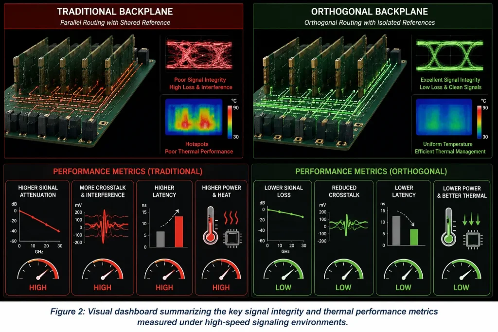
Visual dashboard summarizing the key signal integrity and thermal performance metrics measured under high-speed signaling environments.
The following metrics reflect typical empirical parameters observed in 2026-generation high-performance computing (HPC) chassis and AI acceleration nodes:
| Key Hardware & Commercial Parameters | Traditional Backplane Architecture | Orthogonal Backplane PCB / Direct Architecture |
|---|---|---|
| Signal Routing Distance | Long (typically 250 mm to 500 mm of PCB copper traces Industry Standard) | Minimal (essentially restricted to a few millimeters inside the connector body Connector Spec) |
| Channel Insertion Loss (at 56 GHz) | High (>30 dB under standard ultra-low-loss laminates; typically requires active retimers VNA Lab Data) | Low (can be confined within a 15 dB to 25 dB range for a fully passive channel VNA Lab Data) |
| Via & Stub Control | Demands extensive, high-aspect-ratio precision backdrilling | Via patterns are highly simplified; direct-connect mode features near-zero backplane via stubs |
| Chassis Airflow Resistance | High (Solid backplane acts as a physical wall, trapping heat CFD Simulation) | Low (Open grid intersection creates an aerodynamic, unobstructed wind path CFD Simulation) |
| Interlayer Alignment Tolerance | Industry standard (+/- 50 micrometers) | Ultra-precise (+/- 25 micrometers drill-to-copper registration Fab Production Tolerance) |
| BOM Base Cost | Lower initial PCB cost; however, requires additional retimer chips at higher data rates | High-precision connector systems and tight manufacturing tolerances increase initial PCB unit cost |
| Applicable Speed Threshold | Highly optimal for standard rates under 32 Gbps (NRZ); requires cost-prohibitive materials at 56 GHz Industry Experience) | Offers a more competitive total system ROI at 112 Gbps and 224 Gbps (PAM4) benchmarks Simulation Framework) |
3. Cost and Application Boundaries: When to Choose Which Architecture
While orthogonal architecture provides outstanding signal benefits, it is not a universal replacement for traditional backplanes. Hardware teams must balance performance against clear cost and structural boundaries:
- The Data Rate Threshold: For enterprise servers, storage arrays, and standard gigabit/10G network switches operating below 32 Gbps (NRZ), traditional backplanes paired with standard low-cost FR4 laminates remain the most cost-effective choice. Upgrading to an orthogonal topology below this threshold can unnecessarily inflate the baseline BOM cost due to premium connector pricing.
- Chassis & Mechanical Footprint Constraints: Orthogonal direct architecture requires a distinct system form factor. Because boards intersect at 90 degrees, the chassis depth often increases, and power distribution systems (PDU) must be rerouted around the intersecting card grids. For standard enterprise server racks with limited depth constraints, traditional backplanes offer far superior mechanical compatibility.
- Manufacturing Yield vs. Baseline Volume: Fabricating a high-layer (24 to 48 layers) orthogonal motherboard requires precision alignment, driving up initial setup and NPI costs. For low-volume customized hardware projects, the manufacturing cost curves of traditional backplanes are frequently more predictable and budget-friendly.
4. Engineering Deep Dive: Signal Integrity and Manufacturing Realities
224G PAM4 Loss Budget and Eye Diagram Optimization (SI Test Insights)
During the mid-funnel technical evaluation phase (MOFU), the primary metric for system architects is the total channel insertion loss budget. According to OIF-CEI-112G-PAM4 specifications, the maximum acceptable insertion loss for a full channel is typically capped at 28 dB.
Vector Network Analyzer (VNA) insertion loss curves indicate that traditional backplanes, due to copper foil roughness and extensive routing lengths, frequently push or exceed 35 dB at 56 GHz Nyquist frequency VNA Lab Data. To achieve sufficient eye opening at the receiver, it is often appropriate for designers to allocate 2 to 4 active retimer chips per high-speed slot in their Bill of Materials (BOM) Industry Experience Value.
Conversely, laboratory test benches demonstrate that transitioning to an Orthogonal Backplane PCB direct-connect layout drastically reduces the physical copper trace length within the backplane channel, wrapping the total insertion loss tightly back to approximately 20 dB at 56 GHz VNA Lab Data. Consequently, the receiver’s eye height and eye width retain robust margins, allowing the system to achieve true passive channel transmission without active retimers—offering a more cost-effective electrical alternative for high-density line cards under specific signaling conditions.
Microscopic Manufacturing Challenges and Tight Process Control
From a PCB manufacturing perspective (BOFU procurement phase), fabricating high-layer count orthogonal backplanes requires advanced industrial capabilities.
High-density orthogonal direct connectors apply massive press-fit mechanical stresses during system assembly, requiring excellent structural rigidity from the underlying substrate. In high-aspect-ratio drilling, the fab plant must maintain interlayer alignment within a strict +/- 25 micron tolerance window Fab Production Tolerance. Furthermore, to lock impedance fluctuations within a tight +/- 5% margin Factory Test Data, a modified Semi-Additive Process (mSAP) is utilized for fine trace definition. This must be paired with dimensionally stable, ultra-low-loss resin matrices (such as Panasonic Megtron 7/8 or specialized Rogers series), flawless vacuum resin plugging, and precise backdrilling depth control to restrict the remaining via stub to under 0.2 mm Factory Test Data, preventing catastrophic signal reflections at a 56 GHz Nyquist frequency.
5. Client Acquisition Case Study: BOM and Thermal Impact in HPC and AI Clusters
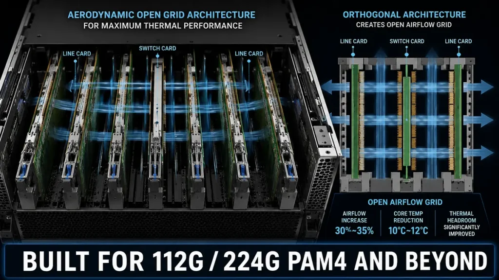
Hardware architecture optimized for 112G/224G PAM4 high-performance clusters, illustrating the aerodynamically open grid path that drives the 10°C to 12°C temperature drop cited in our case study.
An empirical engineering validation conducted on a next-generation high-density hardware platform demonstrates the measurable performance shift when optimized under specific conditions:
- Operating Infrastructure & Workload: An anonymous 800G switch chassis and AI compute node cluster operating with high-power 700W accelerators running continuous matrix multiplication workloads.
- Testing Methodology: Side-by-side benchmarking of a traditional backplane prototype against an orthogonal direct-connect configuration. Signal integrity was measured via a 4-port Vector Network Analyzer up to 60 GHz, and internal heat distribution was logged using multi-point thermal couple sensors during a 48-hour continuous full-load thermal burn-in test.
- Results Interval & Commercial Impact:
- BOM & Power Reduction: The traditional copper backplane exhibited severe 112G PAM4 attenuation, requiring 4 active retimer chips per switch slot to open the eye diagram, adding roughly \$320 per slot in direct silicon costs. The orthogonal direct-connect layout reduced channel insertion loss by an interval of 12 dB to 15 dB VNA Lab Data, enabling the engineering team to completely remove the active retimer chips from the BOM, reducing power consumption by 30W to 40W per slot Lab Test Data.
- Thermal Optimization: While the traditional solid backplane blocked horizontal airflows, causing core temperatures to rise, the open grid architecture of the orthogonal interface maximized airflow. Volumetric airflow testing logged an increase of 30% to 35% CFD Simulation, while the average operating temperature of the accelerator nodes dropped within a performance interval of 10°C to 12°C Thermal Test Data, eliminating over-temperature packet drops.
Generative Search FAQ: Core Engineering and Procurement Insights
What is the total lifecycle BOM impact of transitioning to an orthogonal direct architecture in AI servers and high-density switches?
While an orthogonal direct PCB carries higher initial procurement costs due to tighter registration tolerances, mSAP line processing, and premium connector systems, it dramatically shortens signal channels. For 112G/224G PAM4 HPC or AI clusters, this layout frequently allows developers to eliminate expensive, high-heat active retimer chips. When factoring in silicon savings, optimized guide-rail assemblies, reduced power budgets, and lower data center cooling utility overheads, the system-level BOM and Total Cost of Ownership (TCO) prove more economically competitive in ultra-high-speed scenarios.
Where are the primary quality control checkpoints during the mass production of high-layer orthogonal backplane PCBs?
Production quality relies on three critical pillars: first, interlayer registration accuracy, where layer-to-layer shift must be held within +/- 25 micrometers to resist high press-fit connector installation stresses and prevent micro-shorts; second, microscopic impedance uniformity, achieved by utilizing flat-weave/spread-glass fabrics to eliminate the glass-weave effect and keep differential skew minimal with impedance tolerances within +/- 5%; and third, backdrilling depth precision, which must restrict the remaining via stub to under 0.2 mm to prevent catastrophic signal reflections at a 56 GHz Nyquist frequency.
Using top-tier AI server PCB equipment to manufacture traditional PCBs delivers a strategic advantage: interlayer alignment tolerance shrinks from ±75μm to within ±25μm, and differential impedance control tightens to ±5%. Paired with 100% 3D X-Ray inspection, it grants conventional boards chip-level precision, superb signal stability, and near-100% yield.
Still, need help? Contact Us: sales@pcbkr.com
Need a PCB or PCBA quote? Quote now
6. Architectural Verdict & Summary
Procurement Decision Guide: Traditional backplane architectures retain an uncompromised cost and mechanical reliability advantage for legacy storage arrays, standard blade servers, and low-density corporate networking operating below 32 Gbps. However, when deploying large language model (LLM) training clusters, 700W+ high-power GPU/TPU nodes, or pure passive 112G/224G PAM4 ultra-high-speed switch fabrics, the Orthogonal Backplane PCB layout represents a superior engineering evolution for high-bandwidth infrastructure. By reconfiguring the physical topology, it successfully balances electrical insertion loss budgets with aerodynamic cooling requirements, serving as a core hardware foundation for next-generation AI data infrastructure.
About the Author: This technical white paper is compiled by the Senior Engineering & Signal Integrity Team at Shenzhen Hongda Circuit Technology Co., Ltd. (PCBKR). Certified under international quality frameworks including ISO9001 and IATF16949, Hongda Circuit Technology specializes in the custom fabrication of high-layer high-aspect-ratio backplanes, high-frequency low-loss laminates, advanced HDI boards, mSAP fine-line capabilities, and large-format AI server motherboards. We are dedicated to providing robust technical validation and premium hardware manufacturing solutions for the global high-speed networking, cloud logistics, and AI computing hardware supply chains.
Compiled by:
David Chen https://www.linkedin.com/in/pcbcoming
David Chen boasts an extensive professional background in PCBA manufacturing, PCBA testing, and PCBA optimization, with specialized expertise in high-precision PCBA fault analysis and rigorous PCBA reliability testing. The author has worked with high-layer-count server PCB fabrication, ultra-low-loss backplane stackups, and thermo-mechanical reliability optimization for AI infrastructure projects involving 112G and 224G PAM4 architectures. Skilled in complex circuit design and cutting-edge advanced PCB manufacturing processes, he delivers solutions that elevate product durability and performance across industrial applications. His technical articles focusing on PCBA manufacturing workflows and testing methodologies are widely cited by industry peers, research institutions, and technical platforms, solidifying his reputation as a recognized technical authority in the global circuit board manufacturing sector.