High Frequency PCB Fabrication, Hybrid Multilayer PCB, and Advanced RF PCB Stackup Design
Introduction: The New Demands Reshaping PCB Fabrication in 2026
The printed circuit board industry entered 2026 at an inflection point. AI accelerator cards, millimeter-wave 5G/6G radios, low-Earth-orbit satellite transceivers, and next-generation automotive radar modules are simultaneously setting new performance thresholds for substrate materials, fabrication tolerances, and signal integrity management. Where FR-4 laminate once dominated the vast majority of board builds, engineers in these sectors now routinely specify hybrid multilayer PCB constructions that marry cost-efficient FR-4 cores with precision low-loss dielectrics — a combination that delivers the electrical performance of a full RF board at a fraction of the material cost.
Shenzhen Hongda Circuit Technology Co., Ltd. has specialized in high frequency PCB fabrication service for over a decade. This technical article draws on process data from our engineering teams, published material characterization studies from leading laminate suppliers, and the most relevant 2025–2026 advances in RF PCB stackup design to give engineers, procurement managers, and technical evaluators an authoritative, up-to-date reference for their next high-frequency board project.
Why High Frequency PCB Fabrication Service Requires a Specialized Approach
Standard PCB fabrication processes — tuned for FR-4 at operating frequencies below 1 GHz — break down when applied to substrates such as Rogers RO4350B, Taconic RF-35, Isola I-Tera MT40, or Panasonic Megtron 7. The differences are not cosmetic. They originate in the fundamental material physics of PTFE-based and ceramic-filled laminates.
1. Material Properties That Drive High-Frequency PCB Prototyping Requirements
Dielectric constant (Dk) stability across frequency is the first critical dimension. FR-4 has a nominal Dk of 4.2–4.5 at 1 MHz that drifts measurably as frequency climbs into the GHz range. Rogers RO4350B, by contrast, maintains a tightly characterized Dk of 3.48 ± 0.05 from 100 MHz through 77 GHz — a stability that makes precise impedance calculation possible during RF PCB stackup design. Loss tangent (Df) follows a similar pattern: FR-4 exhibits Df values around 0.020 at 1 GHz, while low-loss materials such as Rogers RO3003G2 or Taconic CER-10 hold Df below 0.003 at 10 GHz, translating directly into lower insertion loss and greater link budget headroom.
Coefficient of thermal expansion (CTE) introduces a second challenge. PTFE-composite laminates expand at roughly 14–17 ppm/°C in the Z-axis, whereas standard FR-4 runs at 50–70 ppm/°C. When these materials are pressed together in a hybrid multilayer PCB, the CTE mismatch generates shear stress at the interface during thermal cycling — a failure mode that requires deliberate compensation in bonding film selection and lamination cycle design.
2, Rogers PCB Fabrication Service: Core Process Differences
Our Rogers PCB fabrication service workflow diverges from standard FR-4 processing at four critical points. First, drilling: PTFE is soft and gummy relative to glass-reinforced FR-4, so conventional drill parameters produce fibrous hole walls, sub-optimal resin smear conditions, and reduced copper-to-barrel adhesion. Hongda employs controlled-depth drilling with low-temperature entry foils and optimized drill geometries qualified for each laminate family. Second, desmear and electroless copper deposition parameters are adjusted to address PTFE’s lower surface energy. Third, lamination uses bonding films rather than standard prepregs wherever the hybrid interface occurs, eliminating glass fiber print-through in the RF layers. Fourth, etch compensation tables are recalculated for each material’s specific copper foil treatment and undercut profile, ensuring trace widths land within the tolerance required for controlled impedance.
Key Capability — Hongda RF Fabrication: Impedance control tolerance: ±5% standard / ±3% premium. Minimum trace/space on RF layers: 3 mil / 3 mil. Laminate families supported: Rogers 4000 series, Rogers 3000 series, Taconic RF/TLY/CER, Isola I-Tera MT40, Megtron 6/7, and FR-4 hybrid combinations. Panel size: up to 21″ × 24″. Layer count: up to 40 layers including sequential lamination builds.
Hybrid Multilayer PCB: Architecture, Applications, and Manufacturing Logic
A hybrid multilayer PCB is a board construction in which at least two electrically distinct dielectric materials are combined within a single laminated stackup. The most common configuration pairs one or two RF-grade layers — typically occupying the outer signal layers or the immediately adjacent inner layers — with FR-4 ground and power planes and digital signal layers in the core. This arrangement confines the expensive, process-intensive RF material to the portions of the board where it is electrically necessary, while the cost-effective FR-4 structure handles thermal mass, mechanical rigidity, and low-frequency routing.
1. FR4 and Rogers Hybrid PCB: Stackup Logic for Real Applications
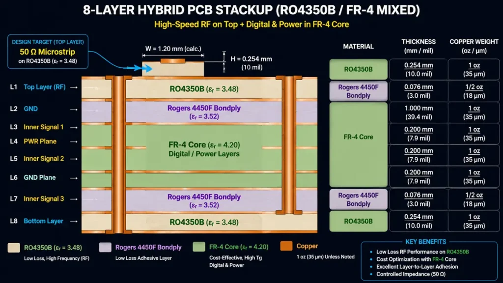
8-Layer Hybrid PCB Stackup Diagram (Rogers RO4350B & FR-4 Mixed Lamination)
The archetypal FR4 and Rogers hybrid PCB in 2026 is an eight-to-twelve layer build serving mmWave radio unit applications. Layer 1 (top) is a Rogers RO4350B signal layer carrying 50 Ω microstrip antenna feeds and LNA input traces. Layer 2 is a continuous copper reference plane — still on RO4350B to maintain tightly controlled microstrip geometry. Layers 3 through N−2 transition to FR-4 or Megtron 6 for intermediate frequency routing, digital control logic, power distribution, and ground planes. Layers N−1 and N (bottom) may return to RO4350B for a second RF interface, or remain in FR-4 if all RF functions are on the top side.
The dielectric boundary between the RF core and the FR-4 core typically uses a Dk-matched bonding film — Rogers 4450F, 2929 bondply, or Taconic FastRise 28 — selected to minimize the electrical discontinuity at the material interface and provide compatible resin flow behavior during lamination. Without careful bonding film selection, resin bleed and voids at the heterogeneous interface compromise both mechanical integrity and signal path consistency.
2. Mixed Dielectric Multilayer PCB Applications in 2026
The range of applications driving mixed dielectric multilayer PCB demand expanded considerably in 2025 and 2026, shaped primarily by four markets:
- AI Inference and Training Infrastructure: High-bandwidth interconnect substrates for GPU and NPU clusters require ultra-low-loss dielectric at 112 Gbps PAM4 signaling rates. Several hyperscale customers have adopted Megtron 7 / FR-4 hybrid constructions to address this without moving to full exotic-laminate builds.
- 5G/6G Sub-6 GHz and mmWave Radio Units (RU): Open RAN radio designs use hybrid boards to separate antenna, PA, and digital baseband functions, each with distinct dielectric requirements, on a single assembly.
- Automotive Radar at 77/79 GHz: ADAS radar sensors are migrating from SiGe modules to PCB-integrated antenna-in-package solutions, where Rogers or Taconic RF material provides the antenna aperture while FR-4 handles the ECU interface and power management circuitry.
- Low-Earth-Orbit (LEO) Satellite User Terminals: Phased-array antenna modules for Starlink competitors use high-layer hybrid PCBs — commonly 16 to 24 layers — with RF material in the antenna and beamforming layers, FR-4 in the digital processing layers, and embedded capacitance in the power distribution planes.
RF PCB Stackup Design: Engineering Fundamentals and 2026 Best Practices
RF PCB stackup design is the engineering discipline that determines the electrical, mechanical, and thermal behavior of a circuit board before a single trace is routed. Stackup decisions — layer sequence, dielectric material selection, copper weight, and plane arrangement — set the ceiling on achievable signal integrity and are extremely difficult and costly to change once a board enters production. The following section presents the structured methodology Hongda’s application engineers use in collaboration with customers during design-for-manufacturability (DFM) reviews.
1. Controlled Impedance RF PCB Design: Setting Target Values Correctly
The most common controlled impedance RF PCB design targets are 50 Ω single-ended (microstrip or stripline) for RF signal lines and antenna feeds, and 100 Ω differential (edge-coupled or broadside-coupled) for high-speed digital pairs. However, selecting the target impedance is only the first step. Achieving it in manufacture requires modeling the actual electromagnetic field distribution across the specific layer stackup using a 2D field solver — tools such as Polar Instruments Speedstack, Ansys SIwave, Keysight ADS substrate editor, or the Sonnet EM planar solver.
A key lesson from production data: nominal Dk values published in material datasheets are measured at a specific frequency (commonly 10 GHz for RF laminates, and 1 MHz for FR-4). The Dk a field solver needs is the value at the operating frequency of the circuit — and for wideband designs, Dk dispersion must be modeled across the full frequency band. Ignoring this can introduce 3–5% impedance error in designs operating above 20 GHz, which translates to measurable return loss degradation at antenna ports.
2. RF PCB Stackup for 5G Applications: Layer Count and Material Selection Guidance
For an RF PCB stackup for 5G applications operating at sub-6 GHz, a four-to-six layer hybrid build is typically sufficient: Rogers RO4350B outer layers (2–4 mil core) bonded to a 4-layer FR-4 core with Rogers 4450F bondply at the interface. For mmWave 5G NR at 28 GHz and 39 GHz, the stackup shifts to an eight-layer design with thinner RF cores — commonly 4 mil thick — to maintain the microstrip line width necessary for 50 Ω on a reasonably wide, etch-controllable trace.
Copper weight matters significantly at mmWave frequencies because of the skin effect: at 77 GHz, current penetrates only approximately 0.27 μm into copper, which means surface roughness of the copper foil — measured as Rz or Rq — directly impacts insertion loss. Reverse-treated foil (RTF) and very-low-profile (VLP) foil grades, available from partners including Olin Brass, Mitsui Mining, and Circuit Foil Luxembourg, have become standard specifications for outer RF layers in Hongda’s premium high frequency PCB fabrication service offering.
3. Microstrip and Stripline Stackup Design: Geometry Tradeoffs
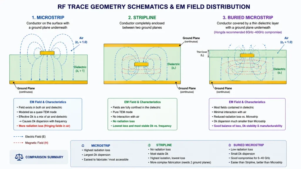
RF Trace Geometries and EM Field Distribution (Microstrip vs. Stripline vs. Buried Microstrip)
Microstrip (signal trace above a single reference plane, exposed to air on one side) has the advantage of easier fabrication access for measurement but suffers from higher radiation loss at mmWave frequencies and more Dk dispersion because the effective dielectric constant is a blend of the substrate material and air. Stripline (signal trace fully embedded between two reference planes) eliminates radiation losses and provides a homogeneous dielectric environment, but introduces manufacturing complexity: the trace cannot be probed without destructive cross-section, and via stub lengths must be managed carefully to avoid resonances within the operating band.
A buried microstrip configuration — signal layer on the inner surface of an outer dielectric layer, with a plane immediately below but the core structure above — offers a useful compromise: the trace is partially enclosed, reducing radiation, while retaining relatively straightforward impedance calculation because the dielectric is still homogeneous above and below. Hongda has standardized buried microstrip as the preferred configuration for RF layers in hybrid multilayer builds when the operating frequency falls between 6 GHz and 40 GHz.
4. EMI/EMC RF PCB Stackup Optimization in Practice
EMI/EMC RF PCB stackup optimization centers on three strategies. First, ensure every RF signal layer has an immediately adjacent, uninterrupted reference plane. A reference plane with slots, cutouts for connectors, or power island splits directly beneath an RF trace creates localized impedance discontinuities and can increase radiated emissions by 10 dB or more. Second, use ground plane stitching vias — placed at λ/20 spacing at the highest operating frequency — to equalize potential between reference planes and suppress parallel-plate resonance between adjacent ground layers. Third, separate analog RF, mixed-signal, and digital sections into distinct zones defined by plane splits and shielding via fences, preventing digital switching noise from coupling into sensitive RF low-noise amplifier inputs.
Advanced Lamination Process for Hybrid PCB Manufacturing
The lamination cycle is the single most consequential manufacturing process step for hybrid multilayer PCB quality. Unlike all-FR-4 builds where process parameters are well-established and tolerant of moderate variation, hybrid lamination involving PTFE-composite and FR-4 materials requires precise control of temperature, pressure, and time — and typically uses a sequential rather than single-cycle approach.
1. Sequential Lamination Strategy for Hybrid PCB Lamination Process
In a sequential lamination strategy, the RF sublaminates are first pressed as individual two-layer or four-layer units at their optimal cure conditions (for Rogers 4000-series: 200°C peak temperature, 200–300 psi consolidation pressure, nitrogen atmosphere). After inspection and inner layer copper plating, these sub-assemblies are then bonded to the FR-4 core layers in a second lamination cycle at the temperatures required for the specific bondply. This staged approach allows each material system to be processed within its own optimal parameter window, preventing the under-cure of bonding resin or the over-consolidation of PTFE that would result from a single universal lamination cycle.
The tradeoff is throughput: sequential builds require additional press cycles, interstage inspection, and handling, adding two to four days to fabrication time relative to a single-lamination FR-4 build. For Hongda customers requiring fast-turn prototype service — our quick-turn HF PCB manufacturing offering — we maintain pre-characterized sub-laminate inventory in standard Rogers and Megtron material combinations to reduce sequential lamination lead time.
2. Bonding Film vs. Prepreg: Selection Criteria for Heterogeneous Interfaces
The choice between adhesive bonding films (Rogers 4450F, Rogers 2929, Taconic FastRise 28, Arlon 6700) and woven glass prepregs (standard FR-4 or high-speed FR-4 such as Isola 370HR) at the RF-to-FR4 interface is determined by three factors. Resin flow must be compatible: prepregs with excess resin flow can encroach into via holes or shift during pressing, while bondplys are formulated for controlled, minimal flow. Second, the glass weave effect — periodic Dk variation caused by the woven glass geometry — is eliminated with non-woven bondplys, improving impedance uniformity for lines that run at arbitrary angles to the weave direction. Third, Dk and Df of the bonding material itself must be factored into the stackup calculation, as it occupies a physically meaningful thickness (typically 2–4 mil) at the material boundary.
3. Void Reduction and Delamination Prevention
Interfacial voids — trapped gas pockets between layers — are a primary reliability failure mode in hybrid builds. Their root cause is usually insufficient resin flow to wet the copper inner layer surfaces before gelation. Hongda addresses this through vacuum-assist lamination (maintaining <10 mbar chamber pressure during the early heating ramp), controlled resin flow characterization of each bondply lot, and a surface preparation protocol for inner copper layers that includes oxide or oxide-alternative treatment for FR-4 surfaces and mechanical scrubbing plus plasma activation for PTFE surfaces.
Precision Impedance Control and High-Density Hybrid Multilayer PCB Fabrication
1. Trace Width Compensation and Etch Factor Management
Controlled impedance fabrication requires that the physical copper trace width achieved after etching falls within a specified tolerance band — typically ±0.5 mil for premium RF work. Because the etching process introduces a characteristic undercut, the artwork trace width must be pre-compensated (widened) relative to the target finished width by an amount that depends on copper weight, etchant chemistry, panel position, and conveyorized etcher speed. Hongda maintains etch compensation lookup tables calibrated quarterly for each combination of copper weight and etchant chemistry on each production line, with test coupon TDR measurements confirming actual impedance vs. modeled target before final customer inspection.
2. Test Coupon Design for S-Parameter and TDR Validation
Every production panel for a controlled impedance build includes at least two sets of test coupons: one on each long edge of the panel. The coupon set includes a 6-inch single-ended 50 Ω microstrip line, a 6-inch 50 Ω differential stripline pair, and a daisy-chain via structure for plated-through-hole resistance verification. Time Domain Reflectometry (TDR) instruments — a Tektronix DSA8300 and a Keysight 86100D in Hongda’s metrology lab — generate impedance profiles from which the process engineer can confirm that the achieved impedance is within customer specification before any panel is released to subsequent operations. For customers requiring RF frequency domain validation, S-parameter measurements up to 20 GHz (network analyzer: Keysight E5063A) are available as an add-on service.
3. High-Density Hybrid Multilayer PCB: Via Structures and Reliability
High-density interconnect (HDI) features — laser-drilled microvias, stacked vias, skip vias — add another dimension of complexity to hybrid multilayer PCB construction. PTFE-based outer layers respond differently to UV laser drilling (355 nm Nd:YAG) than FR-4: PTFE requires lower pulse energy and higher repetition rate, and the resulting microvia wall profile is more tapered than in glass-reinforced substrates, requiring adjusted copper conformal fill parameters in the via fill plating step. For stacked microvia structures landing on buried RF layers, Hongda employs via-in-pad with planarized copper fill, confirmed by cross-section analysis (≥85% fill by SEM cross-section) to ensure reliability through 1,000 thermal cycles per IPC-6012 Class 3 requirements.
Quality Assurance Protocols for High Frequency PCB Fabrication
Quality control in high frequency PCB fabrication service must address both the standard acceptance criteria of IPC-6012 and the additional electrical performance requirements specific to RF substrates. The following protocols are standard at Shenzhen Hongda Circuit Technology Co., Ltd.:
1. Incoming Material Verification
- Dk and Df certificate verification against material lot trace number for every incoming laminate roll.
- Moisture content check: RF laminates are baked at 120°C for 2 hours before pressing to prevent outgassing-induced voids.
- Visual inspection of copper foil surface finish under 50× magnification, with any pitting, scratches, or oxide anomalies triggering lot rejection.
2. In-Process and Final Inspection
- Automated optical inspection (AOI) after inner layer imaging to detect opens, shorts, and line width violations ≥15% of nominal.
- X-ray layer registration check after lamination: ±2 mil maximum registration tolerance between any two signal layers.
- Impedance coupon TDR on every panel before etch, with documented process adjustment if any coupon falls outside ±5% (±3% for premium tier).
- Final electrical test: 100% flying probe continuity and isolation test for prototypes and low-volume orders; dedicated fixture testing for volumes above 50 panels.
- Cross-section metallography: sampled at 1 panel per lot or per customer requirement, verifying copper thickness in vias, interfacial void absence, and dielectric thickness uniformity.
Design for Manufacturability (DFM) in Hybrid High-Frequency PCB Builds
The greatest preventable source of cost and schedule overrun in hybrid multilayer PCB projects is a mismatch between what the schematic and layout intend electrically and what the fabrication process can reliably achieve. Hongda’s DFM review process, conducted at the Gerber and ODB++ review stage before fabrication release, consistently surfaces the following issues:
1. Stackup Validation and Compatible Prepreg Selection
The most common DFM finding in new customer designs is a stackup specification that combines materials whose resin flow and bonding chemistry are incompatible. A typical example: a designer specifies Rogers RO4350B cores bonded with Isola FR408HR prepreg. While this combination is not impossible, it requires extensive characterization and may underperform a build using Rogers 4450F bondply at the same interface. Hongda provides a no-charge stackup validation service in which our applications engineers model the proposed stackup in Polar Speedstack, check material compatibility, recommend bonding film substitutions where needed, and return a revised stackup drawing within 24 hours.
2. Via Design Rules for RF Layers
Unnecessary buried or blind vias in RF signal layers add parasitic inductance and capacitance that can degrade S11 return loss at GHz frequencies. DFM best practice: use through-hole vias with back-drilled stubs wherever via stub resonance would fall within the operating band, and minimize via count in impedance-controlled RF signal paths. For differential pair routing, ensure that both via transitions occur simultaneously (matched via pairs) to prevent mode conversion from differential to common mode at the interconnect.
3. Copper Balance and Board Symmetry
Asymmetric copper distribution — more copper on one side of the board than the other — causes bow and twist after lamination and thermal excursion. For hybrid builds where the RF material has a different CTE than the FR-4 core, copper balance is even more important because thermal mismatch already introduces stress at the material interface. Hongda’s DFM check includes a copper area analysis (target: <10% difference between top half and bottom half of the stackup) and recommends copper fill in unused routing areas of FR-4 layers where needed to restore balance.
Cost Structure and Total Cost of Ownership for High-Frequency PCB Fabrication Service
A realistic understanding of cost drivers in high frequency PCB fabrication service is essential for engineers and procurement managers evaluating supplier quotations and making strategic build-vs-buy decisions.
1. Key Cost Drivers in Rogers PCB Fabrication Service
RF laminate material cost is the largest single variable. Rogers RO4350B laminate runs approximately 8–12× the cost per unit area of standard Tg170 FR-4 at comparable thickness. However, because hybrid multilayer PCB designs confine the RF material to one to four layers within a much larger multilayer stack, the actual RF material fraction of total board cost is typically 25–40%, not 100%. Sequential lamination press cycles add roughly 30–50% to fabrication time cost relative to a single-cycle FR-4 build. Impedance testing, cross-section sampling, and RF frequency validation add a further 5–15% to final inspection cost.
2. How Customers Can Optimize Total Cost
- Minimize RF material layer count: every layer converted from Rogers to FR-4 reduces material cost by 7–10× on a per-layer basis.
- Consolidate RF functions to adjacent layers to enable single-sequential lamination rather than multiple sequential press cycles.
- Specify Rogers 4000-series (thermoset) rather than PTFE-based material where operating frequency permits: thermoset RF laminates are more compatible with standard FR-4 processing, reducing cycle complexity and cost.
- Engage with Hongda’s DFM team before finalizing the stackup: early changes cost nothing; late changes after tooling can add 15–25% to prototype cost.
2026 Technology Trends Driving the Future of RF PCB Manufacturing
1. Ultra-Low-Loss Materials and Emerging Substrates
The materials landscape for high frequency PCB fabrication service continued to evolve through 2025 and into 2026. Rogers introduced the RO4000 LoPro series with enhanced surface roughness control targeting insertion loss reduction above 40 GHz. Panasonic’s Megtron 8 reached commercial qualification at leading Japanese contract manufacturers, offering Dk of 3.2 and Df of 0.002 at 10 GHz in a glass-reinforced form factor that enables standard drill and routing processes. AGC’s ESTERLAM 21 fluoropolymer-composite family gained adoption in European defense and space programs for operation at cryogenic temperatures where PTFE’s dielectric stability is critical.
9.2 AI-Driven Process Automation in PCB Fabrication
Machine learning applications entered PCB fabrication process control in earnest during 2025. Computer vision systems trained on historical AOI datasets now achieve inner layer defect detection accuracy exceeding 99.7% while reducing false-call rates that historically required manual operator review. Etch process control loops using inline X-ray fluorescence measurement of copper thickness — feeding adjustment signals back to the etcher in real time — have reduced impedance variation within a panel from ±8% (manual control) to ±3% (closed-loop AI control) in early adopter fabs. Hongda is currently in the pilot phase of implementing ML-based lamination cycle optimization, using thermocouple data from test panels to adjust heating ramp profiles in real time based on predicted resin flow behavior.
3. High-Layer-Count Hybrid PCB for AI Hardware
The AI hardware market in 2026 is pulling PCB suppliers toward layer counts and routing densities that were considered impractical just three years ago. Switch fabric boards for hyperscale AI training clusters now routinely specify 40-to-50-layer counts with Megtron 7 hybrid construction, embedded planar magnetics, and sub-2-mil trace geometries on inner routing layers. Hongda’s 2026 capability roadmap includes qualification of 50-layer sequential lamination builds and introduction of 1 mil line/space processing on inner layers for customers designing next-generation AI interconnect substrates.
Selecting the Right High Frequency PCB Fabrication Service Partner
Not all PCB manufacturers that claim high-frequency capability have equivalent depth of process knowledge, material qualification, or engineering support. When evaluating a high frequency PCB fabrication service supplier, the following criteria distinguish genuinely capable partners from those with limited hybrid PCB experience:
- Material handling breadth: Can the supplier demonstrate production builds using Rogers, Taconic, Isola, and Megtron families — not just one? Each material family has specific handling, drilling, and bonding requirements that require separate process qualification.
- Impedance control documentation: Does the supplier provide TDR coupon data with every order, or only on request? Is the measurement correlated to specific coupons on your specific panel, or is it a generic process statement?
- DFM capability: Does the supplier have applications engineers who can review your stackup before fabrication and identify material compatibility or via design issues? This service should not cost extra — it reflects process knowledge, not a premium feature.
- Sequential lamination experience: How many sequential lamination builds has the supplier shipped in the past 12 months? Request reference customers in your target application area.
- RF frequency domain validation: Can the supplier measure S-parameters up to the operating frequency of your design, not just TDR impedance?
Hybrid multilayer PCB construction, advanced RF PCB stackup design, and precision high frequency PCB fabrication service represent three interdependent pillars of modern RF and mixed-signal electronics manufacturing. In 2026, the convergence of AI hardware demands, 5G/6G infrastructure buildout, automotive radar proliferation, and LEO satellite deployment has made these capabilities not just a niche specialty but a core requirement for any PCB supplier serving leading-edge electronics markets.
Shenzhen Hongda Circuit Technology Co., Ltd. has invested continuously in the process equipment, material qualifications, engineering talent, and quality systems required to manufacture hybrid RF boards reliably at both prototype and volume production scales. We invite engineers and procurement professionals to contact our applications team for stackup review, design-for-manufacturability consultation, or a quotation on your next high-frequency board project.
FAQs for High-Frequency PCB Procurement
Are your Rogers and exotic laminates 100% authentic, and which low-loss material brands do you support?
Shenzhen Hongda Circuit Technology Co., Ltd. has specialized in high-frequency PCB fabrication for over a decade. Every incoming laminate roll undergoes rigorous material lot trace number tracking and certificate verification for Dk and Df to guarantee 100% authenticity. We support a broad spectrum of industry-leading low-loss materials:
1. Rogers: 4000 and 3000 series (e.g., RO4350B, RO3003G2, and LoPro series).
2. Other Low-Loss Materials: Taconic (RF/TLY/CER series), Isola (I-Tera MT40), and Panasonic (Megtron 6/7/8).
3. Standard Cores: High-Tg FR-4 used for robust hybrid bonding.
How do you prevent delamination and board warping in FR-4 and Rogers hybrid multilayer PCBs?
Combining PTFE/ceramic-filled laminates with FR-4 is highly prone to shear stress and delamination due to the mismatched Coefficient of Thermal Expansion (CTE). We mitigate this via a three-fold strategy:
1. Sequential Lamination Strategy: We press the RF sublaminates first under their own optimal cure conditions (e.g., 200°C peak temperature for Rogers 4000) before a second press cycle bonds them to the FR-4 core. This prevents under-curing.
2. Advanced Bonding Selection: We utilize Dk-matched, controlled-flow bonding films like Rogers 4450F, 2929 bondply, or Taconic FastRise 28 at the heterogeneous interface instead of generic prepregs to eliminate voids.
3. Surface & Copper Balance: We enforce mechanical scrubbing and plasma activation on PTFE surfaces to maximize adhesion, alongside a rigorous DFM copper-balance check (<10% area variation between layers) to prevent warp.
How much cost savings can we expect by choosing a hybrid multilayer PCB over a full RF board build?
Raw RF laminates like Rogers RO4350B run approximately 8 to 12 times the cost per unit area of standard Tg170 FR-4.
1. By executing a hybrid stackup design, we confine the premium low-loss material only to the outer signal layers where critical RF/high-speed lines are routed.
2. The internal ground, power, and low-frequency routing layers are substituted with cost-effective FR-4. This limits the expensive RF material fraction to just 25% to 40% of the total board cost, providing full RF performance at a massive overall material markdown.
What is your precision impedance control tolerance, and what testing data is delivered with the order?
Ultra-high-speed signaling (such as 112G PAM4 and mmWave RF) leaves no room for trace width error. Our metrology capabilities include:
1. Impedance Tolerance: ±5% standard, down to ±3% premium tier.
2. TDR Coupon Testing: Every production panel includes localized test coupons. We ship a documented Time Domain Reflectometry (TDR) impedance profile report generated by our Tektronix DSA8300 or Keysight 86100D systems with every delivery.
3. Frequency Domain Validation: For designs operating up to 20 GHz, we offer S-parameter frequency testing using a Keysight E5063A network analyzer as an add-on validation service.
About Author
David Chen https://www.linkedin.com/in/pcbcoming
David Chen boasts an extensive professional background in PCBA manufacturing, PCBA testing, and PCBA optimization, with specialized expertise in high-precision PCBA fault analysis and rigorous PCBA reliability testing. The author has worked with high-layer-count server PCB fabrication, ultra-low-loss backplane stackups, and thermo-mechanical reliability optimization for AI infrastructure projects involving 112G and 224G PAM4 architectures. Skilled in complex circuit design and cutting-edge advanced PCB manufacturing processes, he delivers solutions that elevate product durability and performance across industrial applications. His technical articles focusing on PCBA manufacturing workflows and testing methodologies are widely cited by industry peers, research institutions, and technical platforms, solidifying his reputation as a recognized technical authority in the global circuit board manufacturing sector.