How to Choose the Right High Frequency PCB Substrates: Rogers vs. Taconic vs. Teflon
Introduction: Why 2026 Is a Turning Point for PCB Manufacturing Technology
The global printed circuit board industry is undergoing one of its most significant technical transformations in decades. Driven by the explosive growth of 5G mmWave infrastructure, autonomous vehicle radar systems, artificial intelligence (AI) accelerator boards, and satellite communication hardware, demand for high-performance PCB substrates has reached an inflection point that separates manufacturers capable of meeting next-generation requirements from those that cannot.
At Shenzhen Hongda Circuit Technology Co., Ltd., we have been at the forefront of this transformation — investing in advanced lamination presses, laser direct imaging (LDI) systems, and automated optical inspection (AOI) infrastructure to deliver circuit boards that meet the strictest dielectric constant (Dk) stability, low dissipation factor (Df), and fine-pitch trace tolerances that today’s RF, AI, and aerospace applications demand.
This technical overview consolidates the latest advances in PCB manufacturing as of 2026, with particular emphasis on high frequency substrates, material selection frameworks, stackup engineering, and quality benchmarks. Whether you are an RF hardware engineer selecting PCB materials for a 77 GHz automotive radar module or a procurement manager evaluating HDI PCB suppliers for high-volume AI server backplanes, this guide provides the technical depth and commercial context to support your decision.
High Frequency PCB Substrates in 2026 — Material Science Meets Manufacturing Precision
Among all the decisions that define a high frequency PCB’s performance, material selection is the most consequential. The substrate determines signal integrity across the entire operating frequency range, thermal reliability under high-power workloads, and the physical tolerances achievable during fabrication.
Critical Dielectric Constant (Dk) Stability for RF and mmWave Designs
For RF circuits operating above 10 GHz, and certainly above 24 GHz in 5G mmWave and automotive radar applications, the dielectric constant of the substrate must remain stable across both frequency and temperature. Even a 1% variation in Dk at 77 GHz translates to measurable phase error in beamforming arrays and impedance deviation in transmission lines.
In 2026, the industry benchmark for premium RF substrates requires Dk variation of less than ±0.05 across the 1–40 GHz range. Materials such as Rogers RO4350B (Dk = 3.48 ±0.05) and Rogers RO3003 (Dk = 3.00 ±0.04) remain the dominant choices for base station and automotive radar PCBs. Taconic’s TLX and RF-35 series offer competitive Dk stability with PTFE-based chemistry, particularly suited for applications where ultra-low dissipation factor (Df) is prioritized over cost reduction.
Shenzhen Hongda Circuit Technology Co., Ltd. processes these premium laminates with nitrogen-blanketed lamination cycles to prevent oxidation during high-temperature pressing — a manufacturing detail that directly affects the long-term Dk stability of the finished board.
Low Dissipation Factor PCB Materials and Insertion Loss Control
Dissipation factor (Df, also called loss tangent) is the primary determinant of signal insertion loss in high frequency PCB traces. As operating frequencies climb into the mmWave range above 30 GHz, Df differences between substrate materials become exponentially more significant. A substrate with Df = 0.0037 at 10 GHz (Rogers RO4003C) will exhibit far lower conductor loss than a standard FR-4 alternative (Df ≈ 0.020), resulting in tangibly better signal quality over the same trace length.
The 2026 state of the art in low dissipation factor PCB materials includes ceramic-filled PTFE composites achieving Df values as low as 0.0010–0.0015 at 10 GHz. These materials, including specialized grades such as Rogers RT/duroid 5880 and Taconic CER-10, are now being adopted in satellite communication (Satcom) LNB PCB designs and high-power RF amplifier substrates where every tenth of a dB in insertion loss matters at system level.
Copper Foil Selection — Rolled Copper vs. Electrodeposited (ED) Copper in High Frequency Applications
Often overlooked in substrate selection discussions, copper foil surface roughness has a direct and measurable impact on signal loss above 5 GHz due to the skin effect. At high frequencies, current flows only in a thin surface layer of the conductor, making the micro-roughness of the copper-laminate interface a significant loss mechanism.
Electrodeposited (ED) copper foil, the standard for most FR-4 PCBs, typically exhibits surface roughness (Rz) values of 2.5–5.0 μm. Rolled annealed (RA) copper and low-profile (LP) or very low-profile (VLP) electrodeposited variants reduce this to 0.5–1.5 μm, meaningfully reducing conductor loss at frequencies above 10 GHz.
As of 2026, Shenzhen Hongda Circuit Technology Co., Ltd. sources and processes VLP copper foil laminates for all RF PCBs targeting frequencies above 6 GHz, aligning with the emerging standard across Tier-1 automotive and telecommunications PCB suppliers.
Rogers vs. Taconic vs. PTFE Substrates — 2026 Material Comparison for RF PCB Design
The three dominant substrate families for high frequency PCB design each carry distinct trade-offs in electrical performance, manufacturing complexity, and cost structure. Understanding these differences is essential for making informed material selection decisions at the outset of a hardware project.
Table 1: RF PCB Substrate Comparison — 2026 Reference Guide
| Property | Rogers RO4350B | Taconic RF-35 | PTFE (RT/duroid 5880) |
| Dielectric Constant (Dk) | 3.48 ±0.05 | 3.50 ±0.05 | 2.20 ±0.02 |
| Dissipation Factor (Df) @ 10 GHz | 0.0037 | 0.0018 | 0.0009 |
| Thermal Conductivity (W/m·K) | 0.62 | 0.26 | 0.20 |
| CTE (ppm/°C, x/y) | 14 / 16 | 16 / 18 | 31 / 48 |
| Tg (°C) | >280 | >315 (PTFE) | >260 |
| Processing Complexity | Low–Medium | Medium | High |
| Relative Material Cost | Moderate | Moderate–High | High |
| Typical Application | 5G Base Station, Radar | mmWave Antenna, Aerospace | Satcom, >30 GHz RF |
Evaluating Rogers RO4350B vs. Taconic RF-35 for 5G Infrastructure PCBs
Both Rogers RO4350B and Taconic RF-35 are hydrocarbon ceramic composites offering stable Dk and moderate processing complexity — attributes that make them practical choices for high-volume 5G base station and antenna PCB production. The primary differentiator is dissipation factor: Taconic RF-35 achieves roughly half the Df of RO4350B at 10 GHz, which translates to approximately 0.5 dB lower insertion loss per 10 cm of 50-ohm microstrip trace at 28 GHz.
For most 5G sub-6 GHz applications, this difference is commercially insignificant. However, for 28 GHz and 39 GHz mmWave deployments where signal budgets are constrained, the lower loss of RF-35 can justify the modest cost premium and slightly increased handling care during fabrication.
Thermoset Hydrocarbon vs. PTFE Ceramic Composites — Processing Implications for PCB Manufacturers
The choice between thermoset hydrocarbon substrates (Rogers RO4000 series, Isola I-Tera MT40) and PTFE-based materials (Rogers RT/duroid, Taconic TLX, ceramic-filled PTFE variants) has significant manufacturing implications beyond material cost.
PTFE substrates require specialized drilling procedures using sharp, frequently replaced drill bits to avoid fiber delamination; sodium naphthalene etch or plasma activation prior to via plating for adequate copper adhesion; and controlled lamination profiles to prevent the PTFE matrix from flowing under pressure. These process requirements increase cycle time and scrap rate compared to thermoset alternatives. Shenzhen Hongda Circuit Technology Co., Ltd. maintains dedicated production lines with plasma activation equipment and calibrated lamination press programs for PTFE PCB fabrication, ensuring via reliability and dimensional stability on even the most demanding PTFE designs.
Advanced PCB Stackup Engineering and Hybrid Laminate Design in 2026
Modern high-complexity PCBs rarely use a single substrate material throughout the entire stackup. Cost optimization, thermal management requirements, and the need to combine high-speed digital layers with RF analog sections have driven the widespread adoption of hybrid PCB stackups combining standard FR-4 with premium RF materials.
Hybrid Stackup Manufacturing — Combining FR-4 with High Frequency Laminates
A hybrid stackup typically positions the high-frequency substrate layers — Rogers, Taconic, or PTFE — in the outer or near-outer layer positions where RF signals route, while standard FR-4 or high-speed digital materials (such as Panasonic Megtron 6 or Isola I-Tera MT40) occupy the inner core for cost reduction and via aspect ratio management.
The primary technical challenge in hybrid stackup manufacturing is the coefficient of thermal expansion (CTE) mismatch between materials. Rogers RO4350B exhibits a Z-axis CTE of approximately 32 ppm/°C, while standard FR-4 shows 70+ ppm/°C. During lamination and thermal cycling, this mismatch creates stress at the material interface that, if not controlled through optimized lamination pressure and temperature ramp profiles, can cause delamination or via barrel cracking in high-layer-count builds.
As of 2026, hybrid stackup designs with up to 24 layers combining two or three distinct substrate materials are in regular production at Shenzhen Hongda Circuit Technology Co., Ltd., serving customers in 5G infrastructure, automotive ADAS, and AI server hardware development programs.
HDI PCB Technology — Laser Via Formation and Fine-Pitch Interconnect in 2026
High-Density Interconnect (HDI) PCB technology continues to advance rapidly in 2026, driven by the miniaturization requirements of AI edge computing modules, mmWave antenna-in-package (AiP) integration, and advanced driver assistance system (ADAS) PCBs. The defining feature of HDI is the use of laser-drilled blind and buried microvias with diameters from 75 to 150 μm, enabling finer pitch BGAs, smaller board outlines, and improved signal integrity through reduced via stub length.
Current Shenzhen Hongda Circuit Technology Co., Ltd. HDI capability includes any-layer HDI with stacked and staggered microvia structures, laser drill diameter down to 75 μm, via-in-pad with copper plating and planarization, and land grid pitches compatible with 0.4 mm BGA components — meeting the requirements of high-end AI inference and communication hardware.
Impedance Control and Signal Integrity for High-Speed Digital and RF PCBs
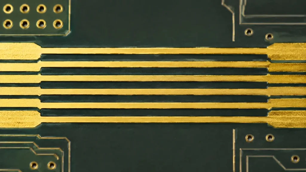
Controlled impedance is non-negotiable in any PCB carrying signals above 1 GHz, and the tolerances required have tightened considerably as data rates have scaled. Where ±10% impedance tolerance was acceptable for early 10G Ethernet designs, current 112G PAM4 links for AI data center switching require ±5% or better, and demanding RF applications specify ±3%.
Achieving these tolerances in production requires tight control of dielectric thickness (±5–8% variation within a panel), copper trace width (±10 μm for outer layers), and surface copper weight after etching. Shenzhen Hongda Circuit Technology Co., Ltd. uses laser direct imaging (LDI) for all high-speed outer layers, eliminating photomask alignment errors that are inherent to traditional film-based imaging, and performs 100% time-domain reflectometry (TDR) testing on controlled impedance boards to verify compliance before shipment.
2026 PCB Manufacturing Technology Advances — What Has Changed and Why It Matters
Additive and Semi-Additive PCB Manufacturing Processes for Fine-Line Traces
Traditional subtractive copper etching processes face fundamental limitations below 50 μm line width due to isotropic etching undercut, making it increasingly difficult to achieve the fine pitch traces required for next-generation RF and AI hardware. In response, modified semi-additive process (mSAP) and additive manufacturing approaches have moved from R&D to limited production in 2025–2026.
In mSAP, a thin seed copper layer (3–5 μm) is laminated, circuits are defined by dry film resist, copper is electroplated to final thickness in defined areas, and the resist and seed layer are stripped — yielding trace widths of 15–30 μm with near-vertical sidewalls. This process, previously limited to package substrates, is now being adopted by advanced PCB manufacturers for AI accelerator boards and 5G mmWave front-end modules requiring sub-50 μm design rules.
Embedded Component PCBs and System-Level Integration Trends
The embedding of passive and active components directly within PCB layers — rather than mounting them on the surface — represents one of the most technically significant manufacturing advances gaining commercial traction in 2026. Embedded component PCBs allow decoupling capacitors to be placed within micrometers of BGA power pins, dramatically reducing parasitic inductance and improving power integrity at frequencies above 1 GHz.
Leading AI hardware companies are now specifying embedded decoupling in their reference designs for AI inference accelerators, and several automotive Tier-1 suppliers have qualified embedded passive PCBs for ADAS domain controller boards. Shenzhen Hongda Circuit Technology Co., Ltd. has established process capability for embedded resistors and capacitors using FR-4 and Rogers-based builds, with ongoing qualification activity for embedded active device integration.
AI-Assisted Design for Manufacturability (DFM) and Automated Engineering Review
One of the most practically impactful changes in PCB manufacturing operations in 2026 is the deployment of AI-powered DFM analysis tools in engineering review workflows. Where a senior process engineer might require 2–4 hours to manually review a complex HDI stackup for potential yield issues, AI-assisted DFM tools trained on historical defect data can flag spacing violations, via-to-copper clearance risks, and hybrid stackup incompatibilities in minutes.
At Shenzhen Hongda Circuit Technology Co., Ltd., AI-assisted DFM review has reduced engineering review turnaround time for complex RF and HDI boards by approximately 60%, allowing us to return detailed feedback to customers within 24 hours of Gerber file submission — a competitive differentiator that accelerates prototype iterations and de-risks production transitions.
Application-Specific PCB Design Considerations — From Automotive Radar to AI Servers
77 GHz Automotive Radar PCB Material Selection and Manufacturing
Automotive radar operating at 77 GHz represents one of the most demanding PCB applications in volume production. At 77 GHz, the free-space wavelength is approximately 3.9 mm, meaning even sub-millimeter trace geometry variations can produce significant impedance discontinuities and pattern distortion in phased-array antenna designs.
Substrate requirements for 77 GHz automotive radar PCBs are unambiguous: Dk values of 2.8–3.2 with stability better than ±0.03 across -40°C to +125°C automotive temperature range; Df below 0.0025 at 77 GHz; low-profile or VLP copper foil; and dimensional stability sufficient to maintain antenna element spacing accuracy through repeated thermal cycling. Rogers RO3003 and Taconic CER-10 are the predominant material choices for this application in 2026.
5G mmWave Antenna Substrates — PCB Requirements for 28 GHz and 39 GHz Infrastructure
5G New Radio (NR) deployment at 28 GHz and 39 GHz frequency bands has driven substantial demand for PCB substrates and manufacturing processes capable of supporting antenna array modules with hundreds of elements. The PCB design requirements for these modules emphasize three properties above all: precise dielectric constant for antenna resonance frequency accuracy; low loss tangent to maximize radiated efficiency; and surface finish uniformity for consistent solder joint quality on the dense RF connector and RFIC attachment points.
Shenzhen Hongda Circuit Technology Co., Ltd. produces 5G mmWave antenna module PCBs in panel formats optimized for automated assembly, with electroless nickel electroless palladium immersion gold (ENEPIG) surface finish as standard for RFIC die attach and wire bond compatibility, and tight bow/twist specifications of less than 0.5% for flatness-sensitive component placement.
High-Speed AI Server PCB — Material and Manufacturing Requirements for 112G PAM4 and Beyond
AI infrastructure buildout in 2025–2026 has generated intense demand for PCBs capable of supporting 112 Gbps PAM4 electrical interfaces and, increasingly, 224 Gbps PAM4 designs targeting next-generation AI switch ASICs and GPU interconnects. At these data rates, the PCB substrate must offer loss characteristics competitive with, or better than, Panasonic Megtron 6 (Df ≈ 0.002 at 10 GHz), with surface roughness and stackup symmetry tightly controlled to minimize differential pair skew and common-mode noise.
The PCB layer count for top-of-rack (ToR) AI switch designs has grown to 32–40 layers in leading designs, with a mix of signal, power, and ground planes demanding advanced impedance-controlled buried and blind via structures. Shenzhen Hongda Circuit Technology Co., Ltd. has qualified 40-layer builds in Megtron 6 and equivalent high-speed dielectric materials, with SI/PI simulation-driven stackup review available as a pre-production service for AI hardware customers.
Quality, Testing, and Reliability Standards at Shenzhen Hongda Circuit Technology Co., Ltd.
IPC Standards Compliance and Beyond — Quality Benchmarks for 2026 RF PCB Production
Quality in PCB manufacturing is defined by adherence to and, in many cases, exceeding IPC Class 3 workmanship and inspection standards — the benchmark for high-reliability applications including telecommunications infrastructure, automotive ADAS, and aerospace electronics. IPC-A-600 Class 3, IPC-6012 Class 3, and IPC-2221 compliance form the baseline quality framework at Shenzhen Hongda Circuit Technology Co., Ltd., applied across all high-reliability product lines.
Beyond standard IPC compliance, customers in automotive programs require IATF 16949-aligned manufacturing process controls, while aerospace customers specify AS9100D quality management system requirements. Shenzhen Hongda Circuit Technology Co., Ltd. maintains certified quality management systems aligned with these standards and provides full first-article inspection (FAI) documentation, including cross-section analysis, copper thickness measurement, and ionic contamination testing on request.
PCB Testing Capabilities — TDR, Insertion Loss Measurement, and Impedance Verification
Verifying the electrical performance of a high frequency PCB requires more than visual inspection. Time-domain reflectometry (TDR) testing is performed on controlled impedance coupons on every panel to verify trace impedance against design specification. For RF boards, insertion loss measurement on dedicated test coupons using vector network analyzer (VNA) equipment provides quantitative validation of substrate performance matching simulation models.
All boards produced for automotive radar, 5G antenna, and satellite communication applications undergo 100% electrical testing (flying probe or bed-of-nails fixture depending on volume), with test coverage including continuity, isolation, and four-wire Kelvin resistance measurement on critical power and ground networks. Thermal cycling and humidity testing per IPC-TM-650 methods are available for reliability qualification samples.
Choosing a PCB Manufacturer for High Frequency Applications — What Engineers and Procurement Teams Should Evaluate
Supplier Capability Matrix for RF PCB Manufacturing in 2026
When evaluating PCB manufacturers for high frequency applications, the following capability dimensions are directly predictive of product quality and project success. Material sourcing — specifically, direct partnerships with Rogers, Taconic, and Isola for premium RF substrate supply — is foundational. A manufacturer without these relationships cannot guarantee authentic material traceability, which is a non-negotiable requirement for automotive and aerospace programs.
Process capability for controlled impedance should be evaluated against actual production data, not theoretical claims. Ask for Cpk data from impedance test coupons on recent production panels, and verify that the claimed tolerance (±5% or better) is consistently achieved in volume, not just on optimized prototypes.
Table 2: PCB Manufacturer Evaluation Criteria for High Frequency Applications
| Evaluation Criteria | Baseline Requirement | Best-in-Class Standard |
| RF Substrate Material Sourcing | Rogers, Taconic available | Direct partnership, full traceability |
| Minimum Trace/Space (Outer Layer) | ≤75/75 μm | ≤25/25 μm (mSAP) |
| Controlled Impedance Tolerance | ±10% | ±3% |
| Microvia Diameter (Laser Drill) | ≤150 μm | ≤75 μm |
| Max Layer Count | 20 layers | 40+ layers |
| TDR Testing | On request | 100% on all controlled impedance boards |
| PTFE PCB Processing Capability | Not available | Dedicated PTFE production line |
| DFM Turnaround | >48 hours | <24 hours (AI-assisted) |
| Quality Certification | ISO 9001 | IATF 16949 + AS9100D |
Why Shenzhen Hongda Circuit Technology Co., Ltd. Is Positioned for 2026 and Beyond
Shenzhen Hongda Circuit Technology Co., Ltd. combines three competitive strengths that are increasingly rare to find in a single manufacturing partner: the technical depth to engage meaningfully with RF and high-speed digital design challenges from the early prototype stage; the process breadth to manufacture across the full spectrum from standard FR-4 multilayer boards to complex PTFE-based hybrid HDI stackups; and the quality infrastructure to meet automotive and telecommunications reliability requirements in production volumes.
Our engineering team provides stackup design assistance, hybrid laminate DFM review, and simulation-driven impedance modeling to customers at no additional charge during the pre-production phase — reducing design iterations and shortening the path from prototype to qualified production release. Whether your next program is a 77 GHz automotive radar module, a 400G AI data center switch PCB, or a custom Satcom terminal hardware build, we invite you to engage with our technical sales team for a design review and manufacturing feasibility assessment.
PCB Technology in 2026 Demands a Manufacturing Partner, Not Just a Supplier
The advances in PCB manufacturing technology documented in this article — from VLP copper foil and PTFE substrate processing to mSAP fine-line fabrication and AI-assisted DFM — represent a widening capability gap between manufacturers equipped for next-generation hardware and those operating on legacy process baselines. For engineers designing RF, mmWave, automotive radar, and AI infrastructure hardware, selecting the right PCB manufacturer is as consequential as selecting the right substrate material.
Shenzhen Hongda Circuit Technology Co., Ltd. has built its manufacturing infrastructure, engineering expertise, and quality systems specifically to serve the demands of technically complex, performance-critical applications. We look forward to demonstrating that capability on your next PCB project.
Contact Shenzhen Hongda Circuit Technology Co., Ltd. for technical consultation, stackup design review, and prototype quotation. Our engineering team responds within 24 hours.
FAQ
What is the primary difference between Rogers and Taconic PCB substrates?
The choice between Rogers and Taconic depends on your specific RF design and processing priorities. Rogers materials, such as the RO4000 series, are hydrocarbon ceramic laminates that behave similarly to standard FR-4 during manufacturing, offering excellent mechanical stability and ease of fabrication. In contrast, many popular Taconic laminates are PTFE-based (Teflon) composites, which provide an exceptionally low dissipation factor (Df) and minimal insertion loss at ultra-high frequencies. However, PTFE substrates require specialized plasma or sodium naphthalene etching for via preparation and demand stricter handling during lamination.
Why is Dielectric Constant (Dk) stability critical for millimeter-wave (mmWave) PCBs?
At high frequencies (such as 28 GHz, 39 GHz, or 77 GHz), the wavelength of the signal is extremely short. Any slight variation in the substrate’s Dielectric Constant (Dk) across the panel or over temperature ranges will alter the electrical path length. This deviation leads to severe phase errors in antenna arrays, reflection loss, and impedance discontinuities in 50-ohm microstrip transmission lines. For premium RF performance, a Dk tolerance of less than ±0.05 is mandatory to ensure signal integrity.
How does copper foil surface roughness affect high-frequency insertion loss?
Due to the “skin effect,” high-frequency currents do not flow through the center of a conductor; instead, they migrate to the outer surface. If the copper-laminate interface is rough (like standard electrodeposited copper with an Rz of 2.5–5.0 μm), the signal path travels a longer physical distance over the micro-peaks and valleys, exponentially increasing conductor loss. Utilizing Very Low Profile (VLP) or rolled annealed (RA) copper foil with a surface roughness under 1.5 μm is essential to minimize insertion loss above 10 GHz.
Can I combine standard FR-4 with high-frequency materials in a hybrid stackup?
Yes, hybrid PCB stackups are widely used in 2026 to balance cost and electrical performance. Typically, premium RF laminates (like Rogers RO4350B or Taconic) are placed on the outer layers where high-speed RF traces are routed, while lower-cost FR-4 or high-speed digital core materials occupy the inner layers. The primary manufacturing challenge is managing the Coefficient of Thermal Expansion (CTE) mismatch between the layers to prevent delamination or via cracking during thermal cycling.
What surface finish is best recommended for high-frequency RF PCBs?
Electroless Nickel Electroless Palladium Immersion Gold (ENEPIG) and Immersion Silver are highly recommended for high-frequency designs. ENEPIG provides an ultra-flat surface ideal for fine-pitch component placement, wire bonding, and high-density RFIC attachments. Immersion Silver provides exceptional electrical conductivity and lower skin-effect loss, though it requires strict handling to prevent surface oxidation before assembly. Standard HASL should be strictly avoided due to its uneven surface profile and high insertion loss.
About Author
David Chen https://www.linkedin.com/in/pcbcoming
David Chen boasts an extensive professional background in PCBA manufacturing, PCBA testing, and PCBA optimization, with specialized expertise in high-precision PCBA fault analysis and rigorous PCBA reliability testing. The author has worked with high-layer-count server PCB fabrication, ultra-low-loss backplane stackups, and thermo-mechanical reliability optimization for AI infrastructure projects involving 112G and 224G PAM4 architectures. Skilled in complex circuit design and cutting-edge advanced PCB manufacturing processes, he delivers solutions that elevate product durability and performance across industrial applications. His technical articles focusing on PCBA manufacturing workflows and testing methodologies are widely cited by industry peers, research institutions, and technical platforms, solidifying his reputation as a recognized technical authority in the global circuit board manufacturing sector.