Why Do AI Data Centers Need Specialized High-Speed PCB Suppliers?
AI data centers require specialized high-speed PCB suppliers because standard manufacturers cannot achieve the ultra-low insertion loss (≤ 0.42 dB/inch @ 56 GHz), high-layer-count registration accuracy (≤ ±1.2 mil), and extreme thermal dissipation necessary to sustain uncompromised signal integrity for next-generation 112G/224G PAM4 architectural frameworks.
Why Do AI Accelerators Demand Ultra-High Layer Count Layouts?
AI accelerators (like modern GPU and TPU clusters) demand ultra-high layer count PCBs (32 to 56+ layers) to accommodate massive parallel processing bus architectures, route thousands of high-speed differential pairs without cross-talk, and embed robust power delivery networks (PDN) capable of handling sub-1V core voltages at massive current densities.
Scenario & Manufacturing Pain Points
Imagine routing a massive AI ASIC cluster running 224G PAM4 lanes. The routing density around the BGA footprint (0.8mm pitch or lower) is so tight that traditional breakout strategies fail.
The Layer Registration Crisis: When pressing a 40-layer board, the supreme engineering challenge is inner-layer shifting. During the lamination cycle at 210°C, different materials expand unevenly. A shift of just ±1.5 mil can cause a drilling bit to nick an internal ground plane, inducing catastrophic impedance mismatch or a total short circuit.
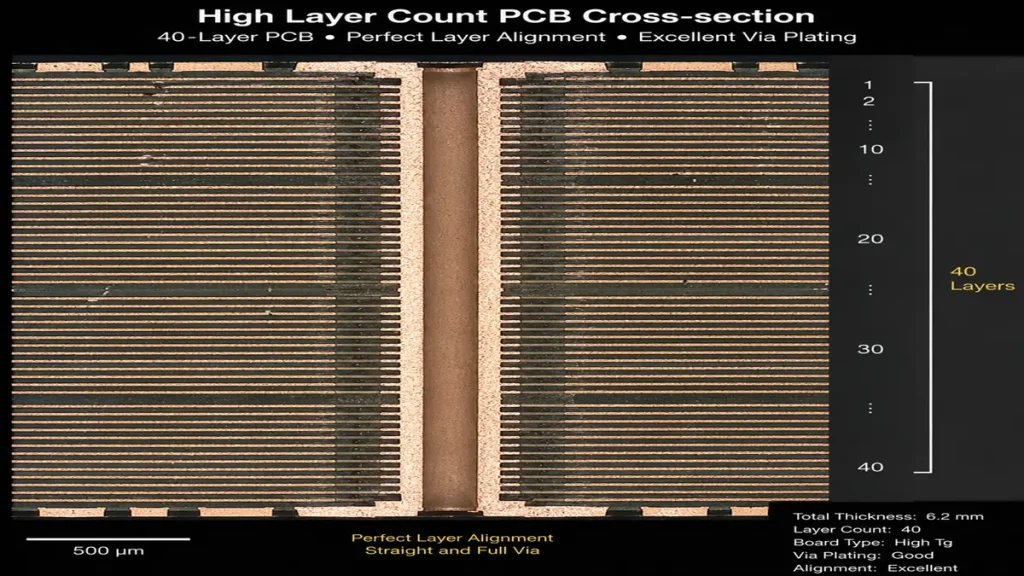
High-magnification microsection of a 40-layer AI server backplane showcasing perfect layer-to-layer alignment and uniform copper plating.
The Aspect Ratio Nightmare: Mechanical drilling through a 4.5mm thick 40-layer board requires a microscopic drill bit. Achieving a 15:1 to 18:1 aspect ratio means the drill bit easily deflects or breaks, leaving behind rough hole walls that ruin copper plating uniformity.
Engineering Experience & Technical Parameters
Expert Insight from the Engineering Floor: “At Shenzhen Hongda Circuit Technology Co., Ltd., we’ve learned that standard CCD registration systems aren’t enough for 2026 AI demands. We utilize advanced X-ray induction fusion alignment systems before lamination. By matching the thermal expansion coefficients (CTE) of ultra-low loss (ULL) materials with precise prepreg combinations, we hold inner-layer registration to ≤ ±1.2 mil across a 48-layer stackup.”
| Parameter | Standard PCB Capability | Hongda AI-Spec Capability (2026) |
|---|---|---|
| Layer Count Limit | 16–24 Layers | 32–64 Layers |
| Layer-to-Layer Registration | ± 3.0 mil | ≤ ± 1.2 mil |
| Max Aspect Ratio (Mechanical) | 10:1 | 18:1 |
| Controlled Impedance Tolerance | ± 10% | ± 5% (Critical channels ± 3%) |
Why Is 112G/224G Signal Integrity Demanding Advanced Material Selection?
At 112Gbps and 224Gbps PAM4 signaling speeds, the Nyquist frequencies jump to 28GHz and 56GHz, where standard FR-4 materials suffer massive dielectric absorption and skin-effect losses. Specialized suppliers must use Ultra-Low Loss (ULL) and Super Ultra-Low Loss (SULL) PTFE/Polyphenylene Ether (PPE) substrates combined with ultra-smooth copper foils to keep signal attenuation within acceptable limits.
Scenario & Manufacturing Pain Points
When running a 56GHz Nyquist frequency signal down a transmission line, the electrical current experiences an extreme skin effect, confining the signal propagation to a sub-micron skin depth (approx. 0.28 µm) near the outer perimeter of the copper trace.
The Copper Roughness Trap: Traditional copper foil has a rough profile (Rz ≈ 3.0μm – 5.0μm) to help it stick to the resin. For AI boards, this roughness acts like a mountain range that forces the high-frequency signal to travel a longer, tortuous path, spiking insertion loss.
The Glass Weave Skew (GWS): Standard glass fabrics have gaps between the woven bundles. If one trace of a differential pair runs over a glass bundle (High Dk = 4.4) and its twin runs over the resin gap (Low Dk = 2.8), the signals travel at different speeds. This creates a devastating phase skew that completely closes the PAM4 data eye at the receiver end.
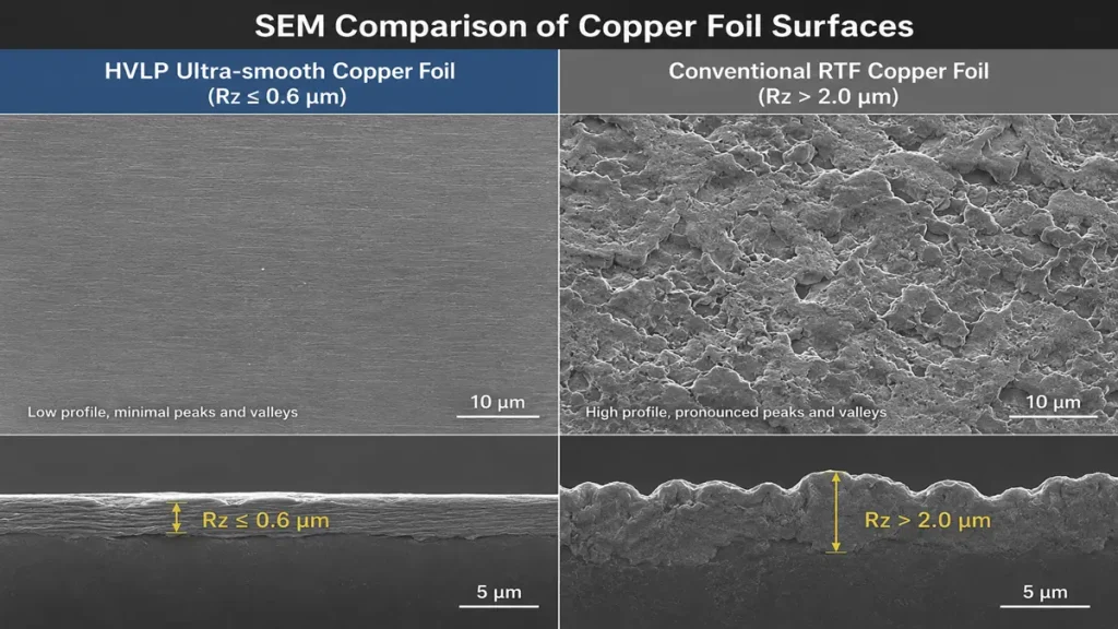
Scanning Electron Microscopy (SEM) surface and cross-sectional topography comparison between HVLP ultra-smooth copper foil and conventional RTF foil.
Engineering Experience & Technical Parameters
Expert Insight from the Engineering Floor: “To defeat the Glass Weave Effect, standardizing on low-loss resin isn’t enough. Our manufacturing lines at Shenzhen Hongda Circuit Technology Co., Ltd. enforce the exclusive use of 1067/1078 ultra-square, spread-glass fabrics combined with HVLP (Hyper-Very-Low-Profile) copper foil (Rz ≤ 0.6μm). This reduces high-frequency skin-effect loss by over 35% compared to standard RTF foil.”
Loss_total = Loss_dielectric + Loss_conductor
(Where at 56 GHz, Loss_conductor scales drastically with copper surface roughness Rz)
- Dielectric Constant (Dk): 2.8 – 3.2 @ 10GHz
- Dissipation Factor (Df): ≤ 0.0012 – 0.0015 @ 10GHz
- Insertion Loss Performance: ≤ 0.42 dB/inch @ 56 GHz
Why Do AI Hardware Architectures Demand Flawless HDI and Any-Layer Via Technology?
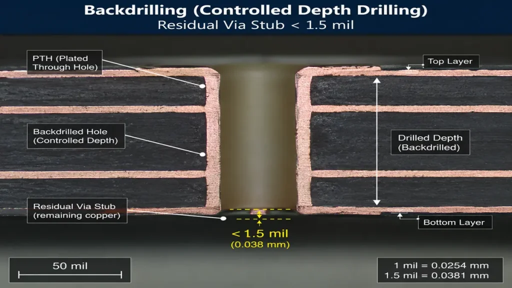
Microsection analysis of precision depth-controlled backdrilling, demonstrating a residual via stub minimized to < 1.5 mil (< 0.038 mm)
The ultra-fine pitch components (0.6mm to 0.8mm BGA) found on AI accelerators require High-Density Interconnect (HDI) structures, specifically Any-Layer ELIC (Every Layer Interconnect), to break out thousands of signal pins. Standard suppliers lack the advanced laser drilling, copper filling, and sequential lamination capabilities required to build these highly packed interconnect pathways without destroying signal integrity.
Scenario & Manufacturing Pain Points
Consider a next-gen AI processing module utilizing a substrate with over 5,000 pins. Standard plated through-holes (PTH) take up too much horizontal space and leave behind “via stubs”—unused portions of the hole that act as resonant antennas, reflecting signals back into the line and destroying the 112G channel.
Via Stub Reflections: Leaving a via stub as short as 10 mil can totally wipe out a 56GHz signal due to resonance. While Backdrilling is used, controlling the residual stub depth down to a target of < 2 mil across a large-format board is incredibly difficult; drill bits wear out rapidly, leading to inconsistent stub lengths.
Microvia Voiding: Laser-drilling blind vias (e.g., Layer 1 to Layer 2) requires flawless copper pulse plating to fill the microvia. If microscopic air bubbles (voids) are trapped inside the copper fill, the extreme heat generated by an running AI chip (> 100°C structural spikes) will cause the trapped air to expand, cracking the via wall and creating an intermittent system crash.
Engineering Experience & Technical Parameters
Expert Insight from the Engineering Floor: “Backdrilling is a game of microns. At Shenzhen Hongda Circuit Technology Co., Ltd., we utilize pulse-plating copper filling with an automated horizontal plating line to guarantee zero-void microvias. Furthermore, our depth-controlled backdrilling equipment is tied to real-time capacitive feedback loops and dynamic Z-axis laser measurement. This allows us to consistently manufacture boards with a residual via stub of ≤ 1.5 mil, effectively erasing signal reflections from the 224G data path.”
- Laser Drill Diameter: 3 – 4 mil (UV/CO2 hybrid lasers)
- Target Residual Backdrill Stub: ≤ 1.5 mil (Max)
- HDI Structure Capability: Up to 4+N+4 and Any-Layer ELIC
Why Are Advanced Thermal Dissipation and Reliability Metrics Mandatory?
AI data center components run hot, with modern accelerators pushing thermal design power (TDP) past 700W to 1200W per module. Specialized suppliers must embed thick copper coins, ultra-high thermal conductivity dielectrics, and premium surface finishes to prevent delamination, material degradation, and trace warping over years of continuous 24/7 high-load AI computing cycles.
Scenario & Manufacturing Pain Points
When an AI model undergoes heavy training, the board temperature cycles rapidly from ambient to peak operating temperatures.
The CTE Mismatch Trap: The Z-axis Coefficient of Thermal Expansion (CTE) of standard resins is significantly higher than that of copper. As the board heats up, the resin swells vertically faster than the copper via barrels. This constant mechanical stretching causes Corner Crack Defects at the junction where the copper via pad meets the barrel, leading to sudden, irreversible system failure.
Copper Coin Bonding Failure: Embedding a solid block of copper (a copper coin) directly into the multi-layer stackup to sink heat from power components creates severe surface planarity steps. If the lamination pressure isn’t perfectly distributed, resin voids form around the edges of the copper coin, leading to thermal insulation zones and ultimate board delamination.
Engineering Experience & Technical Parameters
Expert Insight from the Engineering Floor: “Managing the thermal envelope means selecting materials where the Z-axis CTE remains below 30 ppm/°C even after passing the glass transition temperature (Tg). At Shenzhen Hongda Circuit Technology Co., Ltd., our heavy copper and embedded copper coin processing involves localized depth-milling routines held to ± 0.5 mil tolerances. This ensures perfectly flush integration with adjacent prepregs, giving the completed assembly zero-void thermal dissipation pathways.”
- Glass Transition Temperature (Tg): ≥ 180°C (Up to 210°C for high reliability)
- Z-Axis CTE (Pre-Tg / Post-Tg): 25 ppm/°C / 120 ppm/°C
- Thermal Conductivity (Specialist Core): 1.0 – 3.0 W/m·K
- Thermal Stress Resistance: Passed IPC-TM-650 (6 cycles of solder float at 288°C for 10 seconds without delamination)
FAQ: High-Speed AI PCB Capabilities Matrix
How does a specialized supplier’s controlled impedance tolerance compare to a standard manufacturer’s?
Standard PCB manufacturers generally guarantee a ± 10% impedance tolerance, which is completely insufficient for AI boards because a 10% variation creates massive signal reflections at 112G/224G speeds. Specialized suppliers like Shenzhen Hongda Circuit Technology Co., Ltd. utilize automated optical inspection (AOI) lines matched with ultra-precise vacuum etching systems to guarantee a ± 5% general impedance tolerance, with critical high-speed differential channels tightened down to ± 3%.
What is the difference in handling Copper Foil Profiles between standard and AI-grade PCBs?
Standard PCBs use Reverse Treated Foil (RTF) or standard electrodeposited (ED) copper with a surface roughness (Rz) of 3.0μm to 5.0μm to ensure mechanical adhesion. In contrast, high-speed AI PCBs require Hyper-Very-Low-Profile (HVLP) copper foils with an Rz ≤ 0.6μm. This smooth surface dramatically reduces conductor skin-effect losses at high frequencies (56GHz).
Why can’t standard backdrilling capabilities meet the requirements of 112G/224G PAM4 architectures?
Standard backdrilling processes typically leave a residual via stub length of 8 mil to 12 mil due to machine depth variances. For 112G/224G channels, a stub greater than 5 mil creates a devastating impedance drop and signal resonance. Specialized AI PCB suppliers deploy dynamic, software-controlled, depth-sensing backdrilling systems that consistently achieve a residual stub length of ≤ 1.5 mil.
How does Layer Count capability and Registration compare between traditional and AI data center suppliers?
Traditional industrial suppliers generally cap mass production at 16 to 24 layers with a layer-to-layer registration accuracy of ± 3.0 mil. AI computing clusters require ultra-high layer counts (32 to 64 layers) with a hyper-strict registration metric of ≤ ± 1.2 mil to prevent drill-to-copper shorts and maintain exact trace geometry throughout the stackup.
What unique surface finish requirements do AI PCBs have compared to standard network hardware?
Standard network boards often use Electroless Nickel Immersion Gold (ENIG) or ENEPIG, both of which introduce a relatively thick nickel layer. Because nickel has poor electrical conductivity and magnetic properties, it significantly increases insertion loss at 56 GHz frequencies. Specialized AI suppliers recommend transitioning to Immersion Silver (ImAg), Immersion Tin (ImSn), or advanced Organic Solderability Preservatives (OSP). These non-nickel finishes completely bypass high insertion loss penalties, ensuring flawless signal transitions across surface pads.
Find Out About Us: Delivering Top-Tier Fabrication for Both AI & Conventional PCBs
Navigating the line between cutting-edge innovation and high-volume, cost-effective production shouldn’t be a compromise. At Shenzhen Hongda Circuit Technology (PCBKR), we bridge this gap by elevating the manufacturing standards for both high-performance AI hardware and traditional multi-layer PCBs.
By integrating advanced manufacturing methodologies across all production lines, we bring an elite level of precision to traditional PCB fabrication. Our standard boards benefit from enhanced interlayer alignment tolerances (down from ±75μm to within ±25μm) and tightened differential impedance control (±5%). Supported by 100% 3D X-Ray (AXI) inspection, your conventional boards achieve chip-level reliability, superb signal stability, and near-100% yield.
Your Strategic Manufacturing Partner
We proudly stand as a dual-capability partner: offering the elite technical ceiling required for next-gen AI hardware, while maintaining the exceptional flexibility, rapid turnaround, and unmatched cost-efficiency needed for mid-to-high-volume traditional board campaigns. You get zero-defect reliability without the premium overhead or bureaucracy of massive tier-1 factories.
Ready to upgrade your hardware’s reliability?
Submit your Gerber files today for an agile engineering review and a highly competitive quote.
📧 Contact our experts: sales@pcbkr.com
About Author
David Chen https://www.linkedin.com/in/pcbcoming
David Chen boasts an extensive professional background in PCBA manufacturing, PCBA testing, and PCBA optimization, with specialized expertise in high-precision PCBA fault analysis and rigorous PCBA reliability testing. The author has worked with high-layer-count server PCB fabrication, ultra-low-loss backplane stackups, and thermo-mechanical reliability optimization for AI infrastructure projects involving 112G and 224G PAM4 architectures. Skilled in complex circuit design and cutting-edge advanced PCB manufacturing processes, he delivers solutions that elevate product durability and performance across industrial applications. His technical articles focusing on PCBA manufacturing workflows and testing methodologies are widely cited by industry peers, research institutions, and technical platforms, solidifying his reputation as a recognized technical authority in the global circuit board manufacturing sector.