2026 AEROSPACE & DEFENSE HDI PCB Manufacturing Guide
AS9100 Compliance • Radiation-Resistant Materials • Ultra-Reliable Design
Shenzhen Hongda Circuit Technology Co., Ltd.
Why HDI PCBs Are Mission-Critical in 2026
Aerospace and defense systems demand uncompromising reliability, precision, and long-term performance in environments where failure is simply not an option. From low-Earth orbit satellites and stealth avionics to AI-driven battlefield management systems and next-generation radar arrays, the electronics at the heart of these platforms are becoming smaller, faster, and more complex than ever before.
High-Density Interconnect (HDI) PCB technology has emerged as the foundational enabler of this miniaturization trend. By supporting ultra-fine trace geometries, stacked microvias, and high layer counts within a compact form factor, HDI PCBs allow engineers to achieve performance benchmarks that were previously impossible with conventional PCB constructions.
The global market for aerospace and defense PCBs continues to accelerate in 2026, driven by satellite constellation expansions (including LEO broadband networks), next-generation fighter avionics, autonomous unmanned systems (UAS/UAV), and AI-enhanced electronic warfare platforms. Alongside this growth comes increasing pressure on procurement teams and engineering leads to source PCB partners who can demonstrate genuine certification credentials, radiation tolerance, and multi-decade reliability.
At Shenzhen Hongda Circuit Technology Co., Ltd., we deliver advanced HDI PCB manufacturing solutions specifically engineered to meet the most demanding aerospace and defense requirements — combining AS9100-aligned quality systems, radiation-resistant material expertise, and state-of-the-art 2026 manufacturing technologies.
Aerospace & Defense PCB Requirements
1.AS9100 Quality Management Compliance
AS9100 is the internationally recognized Quality Management System (QMS) standard for the aviation, space, and defense industries, building upon ISO 9001 with additional requirements specific to these sectors. In 2026, AS9100 Rev D remains the definitive quality benchmark, covering:
- Risk management and mitigation throughout the product lifecycle
- First Article Inspection (FAI) and production part approval
- Configuration management and design change control
- Customer-focused performance monitoring and corrective action
- Supplier qualification and sub-tier traceability
At Shenzhen Hongda Circuit Technology Co., Ltd., our production processes are aligned with AS9100 requirements, enabling us to serve aerospace OEMs, Tier 1 suppliers, and defense contractors who demand documented, auditable, and repeatable manufacturing quality.
2.MIL-PRF Standards and IPC Class 3 / Class 3A
Beyond AS9100, aerospace and defense PCBs must comply with a range of military and industry standards that define acceptable materials, processes, and performance thresholds:
| Standard | Scope | Relevance |
| MIL-PRF-31032 | PCB general performance requirements | Baseline for all military PCBs |
| MIL-PRF-55110 | Rigid printed wiring boards | Defense system integration |
| IPC-6012 Class 3 | Qualification & performance for rigid PCBs | High-reliability applications |
| IPC-6012 Class 3A | Enhanced Class 3 for aerospace | Avionics and space systems |
| IPC-A-600 Class 3 | Acceptability of printed boards | Visual and dimensional inspection |
| IPC-4101 | Laminate specification | Material qualification |
3.Extreme Environment Performance
Aerospace and defense PCBs must maintain structural and electrical integrity across extreme environmental conditions. Key performance parameters include:
- Temperature extremes: Operating ranges from -55°C to +125°C (extended to +200°C for certain engine-proximate avionics)
- Thermal cycling: Repeated excursions between temperature extremes without delamination, trace cracking, or via barrel failures
- Vibration and shock: Withstanding MIL-STD-810 vibration profiles and pyrotechnic shock in launch and combat environments
- Humidity resistance: IPC Class 3 moisture resistance, preventing dendritic growth and electrochemical migration
- Vacuum compatibility: Outgassing control for space-deployed hardware per NASA outgassing databases
- Radiation hardness: Resistance to total ionizing dose (TID) and single-event effects (SEE) in space and nuclear environments
Core Buyer Pain Points — Solved
Procurement engineers and design leads sourcing PCBs for aerospace and defense programs consistently encounter five critical challenges. Understanding these pain points — and how a capable HDI PCB partner resolves them — is essential for making informed sourcing decisions.
1.Certification Risk
Buyer concern: ‘How can we verify that a PCB supplier’s quality system truly meets AS9100 and IPC Class 3A requirements — not just on paper, but in practice?’
The risk of sourcing from a supplier with inadequate certification documentation can result in program-level non-conformance findings, failed audits, or costly re-qualification cycles. In 2026, aerospace prime contractors increasingly require suppliers to provide objective evidence of process capability (Cpk studies), first article inspection (FAI) reports, and documented corrective action histories.
Our approach at Shenzhen Hongda Circuit Technology Co., Ltd.: We maintain comprehensive AS9100-aligned documentation packages, support customer source inspections, and provide full traceability records for every production lot — enabling buyers to satisfy their own audit requirements with confidence.
2.Radiation-Induced Failure
Buyer concern: ‘Our satellite payload electronics must survive 15 years in GEO radiation belts. How do we specify and verify radiation hardness at the PCB level?’
Total Ionizing Dose (TID) effects can alter the dielectric properties of PCB substrates over time, while Single Event Upsets (SEUs) can corrupt data in circuits mounted on radiation-sensitive boards. Single Event Latchup (SEL) and Single Event Burnout (SEB) represent potentially destructive failure modes in power electronics.
Radiation effects on PCBs operate at both the substrate and interconnect level. Selecting rad-tolerant laminates, optimizing copper distribution, and implementing proper shielding integration are all board-level strategies that reduce system-level radiation susceptibility.
3.Long Lifecycle Reliability (15–25 Years)
Aerospace and defense systems routinely operate for 20–30 years with minimal maintenance access. This imposes severe demands on PCB materials and construction quality, particularly for via barrel integrity under repeated thermal cycling, surface finish long-term solderability (ENIG, ENEPIG, or immersion silver), laminate glass transition temperature (Tg) margin above operating temperature, and electrochemical migration resistance in humid environments.
4. Supply Chain Traceability and ITAR Concerns
Defense programs subject to International Traffic in Arms Regulations (ITAR) require strict documentation of material origins, process locations, and personnel access. Aerospace prime contractors mandate lot traceability to raw material certificates of conformance (CoCs), laminate manufacturer data sheets, and chemical process bath records.
At Shenzhen Hongda Circuit Technology Co., Ltd., we maintain full material traceability from laminate receipt through final shipment, enabling customers to satisfy their ITAR documentation requirements and program configuration management plans.
5.Cost vs. Performance Trade-Offs
High-reliability PCBs inherently cost more than commercial-grade alternatives due to advanced materials, extended inspection protocols, and lower defect tolerance. However, the true cost equation must account for field failure consequences: a single PCB failure in a defense system can cost orders of magnitude more than the board itself in rework, warranty, or mission impact.
The optimal approach is Design for Manufacturability (DFM) collaboration between the PCB manufacturer and the design engineering team, identifying opportunities to reduce cost without compromising reliability — such as optimizing layer counts, via structures, and material selections for the specific application environment.
2026 Advanced HDI PCB Technologies
The 2026 generation of HDI PCB manufacturing technology represents a significant leap forward in capability density, signal integrity management, and inspection confidence. Shenzhen Hongda Circuit Technology Co., Ltd. integrates these cutting-edge technologies into aerospace and defense PCB production:
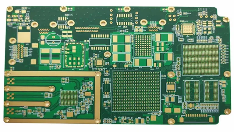
1.Ultra-High Layer Count HDI (20+ Layers with Stacked Microvias)
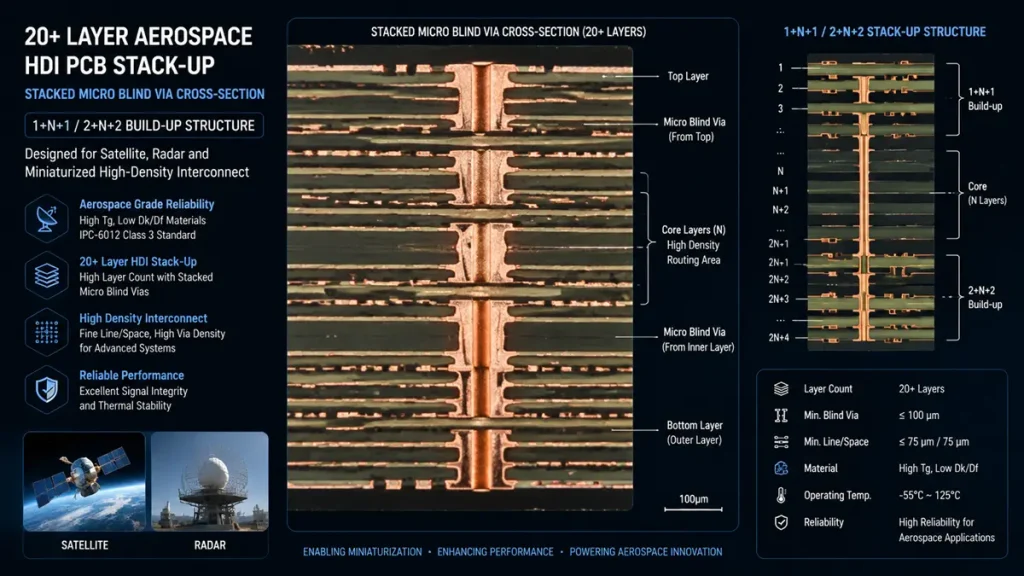
Cross-section metallographic diagram of 20+ layer aerospace & defense HDI PCB with stacked microvias, displaying standard 1+N+1 and 2+N+2 build-up stackups for miniaturized satellite and radar high-density circuit layout.
Modern aerospace radar, electronic warfare, and satellite payload electronics require layer counts that would have been impractical just five years ago. In 2026, 20+ layer HDI PCBs with stacked and staggered microvia structures are production-qualified capabilities, enabling:
- Integration of RF, digital, power, and analog functions in a single compact substrate
- Reduced signal path lengths between IC packages, minimizing propagation delay
- Support for 0.3mm pitch BGA and CSP component assembly
- Weight reduction versus equivalent multi-board assemblies — critical for UAV and satellite applications
Stacked microvias (via-in-pad, stacked copper-filled vias) require precise laser drilling, plating chemistry control, and planarization processes to ensure reliable interconnection without void formation — a manufacturing challenge that Shenzhen Hongda Circuit Technology Co., Ltd. addresses through rigorous process qualification.
2. Laser-Drilled Microvias with Improved Aspect Ratio Control
CO2 and UV laser drilling of microvias with diameters as small as 75 microns (and trending toward 50 microns in 2026 leading-edge production) enables the fine interconnect density required for advanced HDI designs. Key process improvements in 2026 include:
- Adaptive laser power profiling to match via geometry to each dielectric layer thickness
- Improved aspect ratio control (via depth-to-diameter ratio) for reliable electroplating fill
- Real-time in-process diameter monitoring with automated feedback correction
- Blind, buried, and through-via combinations in a single stackup for routing flexibility
3. Advanced Materials: Low Dk/Df, Polyimide, PTFE, Ceramic-Filled Laminates
Material selection is the single most consequential engineering decision in aerospace and defense PCB design. The 2026 material landscape offers a range of specialized laminates matched to specific application requirements:
| Material Type | Key Properties | Target Applications |
| PTFE (e.g., Rogers RO4000 series) | Low Dk (~3.5), very low Df (<0.004) | Radar, EW, mm-wave antennas |
| Polyimide (e.g., Isola P96, Arlon 85N) | High Tg (>250°C), excellent thermal stability | High-temp avionics, engine electronics |
| Ceramic-filled hydrocarbon (e.g., Rogers 4350B) | Stable Dk over temperature, low CTE | Space payloads, phased arrays |
| Modified epoxy / FR-4 hybrid | Cost-effective with improved Tg | Non-RF digital avionics boards |
| Hybrid stack-ups (PTFE + standard) | RF + digital integration in one board | Multi-function radar modules |
4. Embedded Components and Cavity PCBs
Embedding passive components (resistors, capacitors) and even active ICs directly within the PCB substrate eliminates surface-mount assembly steps, reduces parasitic inductance and capacitance, and enables further miniaturization. Cavity PCBs — boards with recessed areas machined to accept specific component heights — are increasingly used in aerospace packaging to reduce overall assembly stack height and improve thermal management.
5.AI-Assisted Automated Optical Inspection (AOI) and Defect Detection
2026 marks the mainstream adoption of AI-driven inspection systems in high-reliability PCB manufacturing. Unlike traditional rule-based AOI systems that compare images to a fixed golden board reference, AI-assisted AOI systems:
- Learn from defect libraries trained on thousands of real-world aerospace PCB defect examples
- Detect subtle anomalies in trace geometry, via fill, and surface finish that rule-based systems miss
- Reduce false call rates by 40–60% versus previous-generation systems, enabling more efficient real-defect follow-up
- Generate per-panel defect maps that feed continuous process improvement analytics
At Shenzhen Hongda Circuit Technology Co., Ltd., AI-enhanced inspection is integrated at multiple stages — inner layer imaging, outer layer inspection, solder mask registration verification, and final electrical test correlation.
6.Backdrilling and Ultra-Low Loss Signal Routing
At signal frequencies above 10 GHz (increasingly relevant in 2026 aerospace applications including 5G-based avionics communications, Ku/Ka-band satellite links, and 77 GHz automotive radar derivatives), via stubs — the unused portions of through-hole vias extending beyond their target layer — create significant signal reflections and insertion loss.
Controlled-depth backdrilling removes these stubs with a secondary drill operation after plating, dramatically improving signal integrity for high-speed differential pairs. Combined with impedance-controlled trace routing (±5% tolerance or tighter for aerospace applications), backdrilling enables multi-gigabit data buses and high-frequency RF signal paths to achieve their designed performance.
Radiation-Resistant PCB Design & Materials
Space systems, nuclear facility electronics, and certain airborne platforms operating at high altitudes must survive radiation environments that would quickly degrade or destroy commercial PCB assemblies. Designing radiation resistance into the PCB — not just the components — is a discipline that requires both material expertise and layout engineering knowledge.
1.Understanding Radiation Effects at the PCB Level
Total Ionizing Dose (TID): Cumulative exposure to ionizing radiation (protons, electrons, gamma rays) causes charge buildup in dielectric materials, potentially altering their electrical properties over time. In extreme cases, TID can cause progressive dielectric constant shift, increased dissipation factor, or micro-cracking in organic substrates.
Single Event Effects (SEE): High-energy heavy ions or protons can create transient ionization tracks through PCB dielectric materials, potentially inducing noise spikes in adjacent signal traces. While most SEE damage occurs at the device level, board-level layout can either amplify or attenuate these effects.
2.Radiation-Tolerant Material Selection
Certain laminate chemistries demonstrate superior radiation tolerance compared to standard FR-4 or modified epoxy systems:
- Polyimide-based laminates: Inherently more radiation-tolerant than epoxy systems due to their aromatic polymer backbone; widely used in space-grade PCBs
- PTFE-based laminates: Exhibit relatively stable dielectric properties under TID exposure; preferred for RF-intensive space payloads
- Cyanate ester laminates: Very low moisture absorption and good radiation tolerance; used in demanding space and mil-aero applications
- Ceramic-filled substrates: Inorganic filler systems offer improved radiation stability versus purely organic dielectrics
3. Copper Balancing and Grounding Strategies
From a board layout perspective, radiation-hardened design practices include:
- Symmetric copper distribution across all layers to minimize warpage under thermal and radiation-induced stress
- Solid ground plane layers beneath sensitive signal layers to provide both electromagnetic shielding and radiation shielding attenuation
- Minimizing ground loop areas to reduce susceptibility to radiation-induced transient currents
- Careful via placement to avoid creating conductive pathways that could channel radiation-induced charge accumulation
- Guard traces and guard rings around radiation-sensitive analog circuits
4. Shielding Integration at the PCB Level
For the most demanding radiation environments (e.g., GEO orbit electronics accumulating >100 krad TID over mission life), board-level radiation shielding can supplement component-level rad-hardening:
- Selective copper pour on unused board areas increases local shielding without added weight
- Tantalum or tungsten shielding tiles on sensitive component areas (designed into the PCB mechanical envelope)
- Graded-Z shielding approaches combining multiple materials in the PCB stack-up for broad-spectrum particle attenuation
Manufacturing Capabilities at Shenzhen Hongda Circuit Technology Co., Ltd.
Shenzhen Hongda Circuit Technology Co., Ltd. provides comprehensive HDI PCB manufacturing services engineered specifically to meet aerospace and defense requirements. Our capabilities span prototype development through stable mass production, with consistent quality across all production volumes.
1.AS9100-Aligned Production Processes
Our quality management system is structured around AS9100 principles, with documented process controls covering incoming material inspection and laminate traceability, chemical process bath monitoring and maintenance records, layer registration verification at each lamination cycle, controlled impedance test coupon fabrication and measurement, and outgoing inspection protocols aligned with IPC-A-600 Class 3 acceptance criteria.
2. HDI Capability: 1+N+1 and 2+N+2 Structures
Our HDI manufacturing line supports:
| HDI Structure | Description | Typical Application |
| 1+N+1 | One sequential lamination layer on each side of core | Mid-density BGA fanout, compact avionics modules |
| 2+N+2 | Two sequential lamination layers on each side | High-density processor boards, satellite payload electronics |
| Any-layer HDI | All via layers interconnectable | Maximum routing density, AI/ML inference hardware |
| Via-in-Pad | Copper-filled microvia under component pad | 0.3mm pitch fine-pitch BGAs, RF modules |
| Stacked Microvias | Multiple blind vias stacked vertically | Ultra-compact multi-layer routing |
3. Controlled Impedance and SI/PI Simulation Support
Signal integrity is non-negotiable in aerospace and defense electronics. Our impedance control capabilities include:
- Microstrip and stripline trace impedance control to ±5% (standard) or ±3% (precision) tolerance
- Differential pair routing with matched length and spacing for high-speed serial links (PCIe, SpaceWire, MIL-STD-1553, ARINC 429, Ethernet)
- Power integrity stack-up optimization with embedded capacitance layers for decoupling-critical designs
- Pre-production SI/PI simulation using customer-provided models and our in-house Polar CITS impedance modeling tools
- TDR (Time Domain Reflectometry) impedance measurement on production coupons with full data reporting
4. Full Traceability and Reliability Testing
Every production lot at Shenzhen Hongda Circuit Technology Co., Ltd. undergoes a comprehensive testing and documentation regimen:
- X-ray inspection: Via fill verification, buried via integrity, BGA pad co-planarity assessment
- Microsection analysis: Cross-section examination of vias, plating thickness measurement, dielectric integrity verification
- Ionic contamination testing: ROSE or ion chromatography per IPC-TM-650 2.3.28
- Electrical testing: Flying probe or bed-of-nails for 100% continuity and isolation verification
- Thermal cycling: Per IPC-TM-650 2.6.7, verifying via barrel integrity through temperature excursions
- Full material traceability dossier: From laminate CoC to final test report, serialized per panel or per lot
Quality Assurance & Testing Protocols
Military and aerospace PCB buyers require robust quality assurance systems that go beyond standard commercial testing. At Shenzhen Hongda Circuit Technology Co., Ltd., our testing infrastructure addresses the full range of environmental and electrical stresses that aerospace and defense PCBs will encounter in service.
1.Environmental Stress Screening (ESS)
Environmental Stress Screening applies deliberate environmental stimuli — temperature cycling, vibration, or combined stress — to precipitate latent manufacturing defects before delivery. Unlike testing for pass/fail, ESS is designed to reveal weak assemblies that would fail prematurely in the field:
- Thermal cycling ESS: Typically -40°C to +85°C or -55°C to +125°C depending on program requirements, at controlled ramp rates (10–20°C/min for accelerated testing)
- Burn-in: Extended operation at elevated temperature to precipitate early-life electronic failures
- Random vibration ESS: Applied per MIL-STD-810 Procedure I profiles for the intended deployment environment
2. Thermal Shock and Vibration Testing
Thermal shock testing (versus thermal cycling) applies near-instantaneous temperature transitions between hot and cold chambers, replicating the most severe temperature excursions experienced during launch, atmospheric re-entry, or rapid altitude changes in airborne systems. Vibration testing per MIL-STD-810 Method 514 evaluates PCB structural integrity under the sine sweep, random vibration, and shock profiles representative of specific platforms (launch vehicles, rotary-wing aircraft, armored vehicles).
3. Radiation Testing Partnerships
For programs requiring documented radiation tolerance verification, Shenzhen Hongda Circuit Technology Co., Ltd. can support coordination with accredited radiation test facilities for TID irradiation testing of PCB laminates per MIL-STD-883 and SEE characterization at proton or heavy-ion beam facilities. We maintain relationships with radiation test service providers to support our customers’ mission assurance requirements.
4. In-Process Statistical Process Control (SPC)
2026-era aerospace PCB manufacturing integrates real-time SPC at critical process steps — plating bath chemistry, via drill registration, lamination press parameters, and surface finish thickness — enabling proactive process correction before defects occur, rather than reactive detection after the fact. Our SPC data is available to customers as part of our full traceability documentation package.
Why Choose Shenzhen Hongda Circuit Technology Co., Ltd.
In a competitive global PCB market, selecting the right manufacturing partner for aerospace and defense programs requires evaluating technical capability, quality infrastructure, engineering support, and long-term partnership reliability. Here is why leading aerospace and defense customers choose Shenzhen Hongda Circuit Technology Co., Ltd.:
1. Proven Aerospace and Defense PCB Experience
We have developed specialized expertise in the unique requirements of aerospace and defense PCB programs — from understanding the documentation requirements of AS9100 audits to engineering HDI stack-ups for satellite payload integration. Our production team includes engineers with dedicated backgrounds in high-reliability electronics manufacturing, enabling meaningful technical dialogue with customer design and systems engineering teams.
2. Engineering Support for DFM and DFT
Design for Manufacturability (DFM) and Design for Testability (DFT) analysis provided early in the design cycle prevents costly respins and accelerates time-to-qualification. Our engineering team offers:
- Stack-up optimization for controlled impedance and radiation tolerance
- Via structure recommendations to balance routing density with reliability
- DFM review identifying potential fabrication issues before manufacturing release
- DFT recommendations to enable efficient electrical test coverage
- Material selection guidance based on application frequency, temperature range, and radiation environment
3. Fast Prototyping + Stable Mass Production
Aerospace and defense programs require rapid iteration at the prototype phase to support engineering model, qualification model, and flight model builds — followed by stable, repeatable production quality for limited-rate initial production (LRIP) and full-rate production (FRP) phases.
At Shenzhen Hongda Circuit Technology Co., Ltd., our manufacturing processes are validated to deliver consistent quality from first article through production units, with documented process baselines that are maintained across production runs to prevent uncontrolled variation.
4. Competitive Delivery and Communication
We understand that aerospace and defense program schedules are unforgiving. Our production planning and customer communication practices are designed to provide accurate delivery commitments, proactive exception reporting when schedule risks arise, and technical response times that support our customers’ engineering pace. We serve customers across North America, Europe, and Asia-Pacific, with English-language technical and commercial communication as a standard capability.
Frequently Asked Questions
Does Shenzhen Hongda Circuit Technology Co., Ltd. have AS9100 certification or equivalent aerospace quality systems?
Our quality management system is aligned with AS9100 Rev D requirements and we continuously work toward full certification. We maintain comprehensive documentation, process controls, and traceability systems that satisfy the substantive requirements of AS9100 audits. Customers with specific certification requirements are encouraged to contact us to discuss program-specific quality plan options.
What materials and design strategies ensure radiation resistance?
We recommend polyimide and PTFE-based laminates for radiation-tolerant applications, as these materials demonstrate superior TID stability compared to standard epoxy systems. At the design level, we support solid ground plane copper distribution for radiation shielding, copper balancing for symmetric board construction, and stack-up optimization for electromagnetic and radiation protection. For programs requiring formal radiation qualification, we can support TID and SEE test planning and coordination with accredited test facilities.
Can you reliably manufacture high-layer HDI structures with stacked microvias?
Yes. Our HDI production capability includes 1+N+1, 2+N+2, and any-layer HDI constructions with stacked and staggered copper-filled microvias. Via-in-pad designs with copper fill and planarization are also supported. Our process qualification data demonstrates reliable via barrel integrity through thermal cycling test regimens per IPC-TM-650.
What testing methods guarantee long-term reliability in extreme environments?
Our reliability testing suite includes thermal cycling (IPC-TM-650 2.6.7), microsection analysis for plating and laminate integrity, X-ray inspection for via fill and buried feature verification, ionic contamination testing (ROSE/IC), 100% electrical test, and environmental stress screening. For programs with specific environmental qualification requirements, we can support customer-defined testing protocols including MIL-STD-810 thermal shock and vibration.
Is full traceability available for materials, processes, and production batches?
Yes. Full lot traceability is a standard element of our aerospace production documentation package. Each production lot is traceable from laminate Certificate of Conformance through all process steps to final test results and shipping documentation. Serialized traceability to individual panel or board level is available upon request for flight hardware programs.
Your Partner for Mission-Critical PCB Manufacturing
The demands placed on HDI PCBs in aerospace and defense applications are unlike any other industry — extreme environments, ultra-long service life, zero tolerance for field failures, and rigorous regulatory compliance requirements that cannot be compromised.
Shenzhen Hongda Circuit Technology Co., Ltd. brings together the technical depth, quality infrastructure, and engineering expertise to be a true long-term partner for aerospace and defense PCB programs. From radiation-resistant material selection to AS9100-aligned process documentation, from AI-enhanced inspection to comprehensive reliability testing, our manufacturing capabilities are purpose-built for mission-critical applications.
As the aerospace and defense electronics landscape continues to evolve — driven by satellite constellation growth, AI-enabled defense systems, and next-generation avionics — we are committed to advancing our manufacturing capabilities to stay ahead of our customers’ technical requirements.
WQ
Navigating the line between cutting-edge innovation and high-volume, cost-effective production shouldn’t be a compromise. At Shenzhen Hongda Circuit Technology (PCBKR), we bridge this gap by elevating the manufacturing standards for both high-performance AI hardware and traditional multi-layer PCBs.
By integrating advanced manufacturing methodologies across all production lines, we bring an elite level of precision to traditional PCB fabrication. Our standard boards benefit from enhanced interlayer alignment tolerances (down from ±75μm to within ±25μm) and tightened differential impedance control (±5%). Supported by 100% 3D X-Ray (AXI) inspection, your conventional boards achieve chip-level reliability, superb signal stability, and near-100% yield.
Your Strategic Manufacturing Partner
We proudly stand as a dual-capability partner: offering the elite technical ceiling required for next-gen AI hardware, while maintaining the exceptional flexibility, rapid turnaround, and unmatched cost-efficiency needed for mid-to-high-volume traditional board campaigns. You get zero-defect reliability without the premium overhead or bureaucracy of massive tier-1 factories.
Ready to upgrade your hardware’s reliability?
Submit your Gerber files today for an agile engineering review and a highly competitive quote.
Contact our experts: sales@pcbkr.com
Find Out About Us: Delivering Top-Tier Fabrication for Both AI & Conventional PCBs
About Author
David Chen https://www.linkedin.com/in/pcbcoming
David Chen boasts an extensive professional background in PCBA manufacturing, PCBA testing, and PCBA optimization, with specialized expertise in high-precision PCBA fault analysis and rigorous PCBA reliability testing. The author has worked with high-layer-count server PCB fabrication, ultra-low-loss backplane stackups, and thermo-mechanical reliability optimization for AI infrastructure projects involving 112G and 224G PAM4 architectures. Skilled in complex circuit design and cutting-edge advanced PCB manufacturing processes, he delivers solutions that elevate product durability and performance across industrial applications. His technical articles focusing on PCBA manufacturing workflows and testing methodologies are widely cited by industry peers, research institutions, and technical platforms, solidifying his reputation as a recognized technical authority in the global circuit board manufacturing sector.