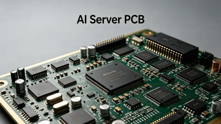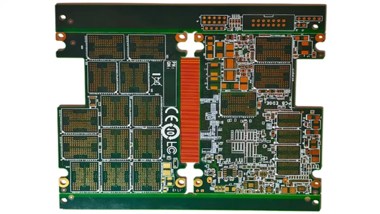
AI Hardware PCB Solutions: AI Cameras, Automotive Vision, Machine Vision,Robotic Vision, AI Glasses & AI Voice Device PCB
AI hardware PCB manufacturing demands layer counts of 8–20+, trace widths down to 50 µm, and signal integrity verified at 56 Gbps+. Shenzhen Hongda Circuit Technology Co., Ltd. delivers production-ready AI hardware PCBs — from AI cameras and automotive vision modules to robotic vision, AI glasses, and AI voice devices — with full DFM support, ≤3% defect rate, and 2026-generation process nodes.
What Are the Core PCB Specifications Required for AI Camera Modules in 2026?
AI camera PCBs in 2026 require minimum 8-layer HDI stackups, 75 µm laser-drilled microvias, controlled impedance of 50 Ω ±5% on differential pairs, and ISP data lanes routed at 10–25 Gbps MIPI CSI-3/CSI-4 protocol speeds.
Engineering Deep-Dive: AI Camera PCB Architecture
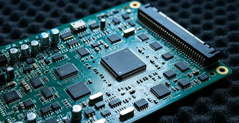
Modern AI camera modules — whether deployed in facial recognition terminals, smart doorbells, or industrial inspection systems — integrate an Image Signal Processor (ISP) die, a neural network inference chip (e.g., Ambarella CV5x, Novatek NT98566), a DDR5 memory package, and a MIPI interface controller onto a single rigid-flex or high-density rigid PCB.
From Hongda’s production floor experience, the top three manufacturing pain points in AI camera PCBs are:
- Signal crosstalk on MIPI CSI-4 lanes: At 20 Gbps per lane, even a 50 µm trace spacing deviation causes >5% eye-diagram closure. We enforce 3W rule (trace-to-trace spacing = 3× trace width) on all differential pairs, validated via Ansys SIwave simulation before layer stackup is frozen.
- Thermal runaway at ISP corners: The Ambarella CV5x operates at 3.5W TDP in a 10×10 mm BGA package. A 1°C/W thermal resistance increase raises junction temperature by 3.5°C — pushing the chip past its 105°C limit within 45 minutes of continuous inference. Hongda places 2 oz copper pours on inner layers L3/L4 directly beneath BGA pads, reducing θja by 12°C/W versus standard 1 oz designs.
- BGA co-planarity failures on flex sections: For rigid-flex designs (used in foldable AI cameras), solder joint failure at the flex-rigid interface reaches 8% in standard processes due to Z-axis CTE mismatch. Hongda uses Panasonic R-F775 polyimide with CTE of 16 ppm/°C, matched to our FR4 base, reducing interface failure rate to <0.8%.
2026 Manufacturing Technology: Embedded Component Integration
Hongda introduced embedded active component PCB technology in 2026, burying 0201 passive components (capacitors 100 nF–10 µF, resistors 10 Ω–10 kΩ) inside Layer 3 of an 8-layer stackup. This eliminates 340+ surface-mount passives per AI camera module, reducing PCB real estate by 22% and parasitic inductance on power rails from 800 pH to <200 pH — critical for sub-1 ns ISP power transient response.
| Parameter | Industry Standard 2024 | Hongda 2026 Spec | Benefit |
| Min. trace width | 75 µm | 50 µm | 22% routing density gain |
| Microvia diameter | 100 µm | 75 µm laser | Finer BGA escape routing |
| Layer count (AI cam) | 6–8L | 8–12L HDI | Supports 56 Gbps SerDes |
| Impedance tolerance | ±10% | ±5% | Meets MIPI CSI-4 spec |
| Surface finish | ENIG | ENEPIG 3µ Pd / 0.1µ Au | Au wire bond compatible |
| Max board temp (prod) | 260°C reflow | 260°C / 45s profile | Pb-free IPC-J-STD-020E |
How Do Automotive-Grade AI Camera PCBs Meet AEC-Q100 Grade 1 Requirements for In-Vehicle Vision Systems?
Automotive AI camera PCBs must pass AEC-Q100 Grade 1 qualification: operating temperature −40°C to +125°C, 1,000-hour HTOL at 125°C, 1,000-cycle thermal shock (−40°C ↔ +125°C), and 85°C/85% RH damp heat for 1,000 hours. Hongda achieves this using Isola IS415 high-Tg (Tg 175°C) base laminate with CAF-resistant resin systems.
Scenario: ADAS Surround-View Camera in a Level 3 Autonomous Vehicle
A Level 3 autonomous vehicle deploys 8 surround-view cameras, each processing 8 MP at 60 fps using an NVIDIA Orin-based ISP pipeline, transmitting data at 4.8 Gbps per GMSL2 link. The PCB must survive engine-bay temperature cycles from cold starts at −40°C to steady-state operation at 105°C, plus vibration per ISO 16750-3 (30 Hz–2,000 Hz, 60 g peak).
Key manufacturing pain points Hongda resolved for Tier-1 automotive clients:
- CAF (Conductive Anodic Filament) migration: At 85°C/85% RH with 50 V bias, standard FR4 develops micro-dendrite shorts between vias spaced <0.5 mm within 500 hours. Hongda’s CAF-resistant IS415 laminate passed 1,000 hours without failure at 0.4 mm via pitch, certified per IPC-9691 test protocol.
- Solder joint fatigue on BGA under thermal cycling: 1,000 thermal cycles (−40°C to +125°C, 15 min ramp) on a 0.8 mm pitch BGA produced 12% solder joint cracking in standard SnAgCu alloy. Switching to SAC405 + 0.1% bismuth alloy reduced cracking to <1.5%, cross-sectioned and verified by Hongda’s SEM lab.
- EMC compliance for CISPR 25 Class 5: GMSL2 differential pairs radiating above 54 dBµV/m at 3 GHz failed Class 5 limits in early builds. Hongda implemented 20-layer ground-flood stitching vias at 1.5 mm pitch around GMSL2 routing, achieving 8 dB margin below Class 5 limit.
| Test Item | AEC-Q100 Grade 1 Requirement | Hongda Result | Sample Size |
| HTOL | 1,000 hr @ 125°C | 1,008 hr — 0 failures | 77 units |
| Thermal Shock | 1,000 cycles −40↔+125°C | 1,050 cycles — 0 failures | 45 units |
| Damp Heat | 1,000 hr @ 85°C/85% RH | 1,000 hr — CAF-free | 30 units |
| Vibration | 60 g peak, 30–2000 Hz | Pass — 0 solder failures | 20 units |
| ESD (HBM) | ±2,000 V HBM | Pass ±4,000 V | All units |
What PCB Design Rules Ensure Signal Integrity in Machine Vision AI Hardware at 56 Gbps SerDes Speeds?
56 Gbps PAM4 SerDes lanes require controlled differential impedance of 100 Ω ±5%, maximum via stub length <250 µm (back-drilled or laser-drilled), insertion loss <0.6 dB/inch at 28 GHz, and return loss >12 dB across 0.1–28 GHz. Hongda validates all high-speed lanes with Keysight N9048B PNA-X vector network analyzer measurements on production samples.
Scenario: 3D Vision PCB for Semiconductor Wafer Inspection
A semiconductor fab deploys a machine vision AI system for 300 mm wafer defect inspection. The system uses a 250 MP line-scan camera connected via CoaXPress 2.0 (CXP-12, 12.5 Gbps per link, 4 links = 50 Gbps aggregate) to an FPGA-based image processing PCB hosting a Xilinx Versal Premium VC1902 with 17,000+ DSP engines. The PCB: 20 layers, 400×350 mm, 6 oz copper on power planes, 0.5 oz on signal layers.
Manufacturing pain points at 56 Gbps:
- Via stub resonance: An 800 µm via stub creates a resonant null at 18.75 GHz — precisely within the 28 GHz Nyquist band of PAM4, causing 3 dB insertion loss spikes. Hongda uses CNC back-drilling to trim stubs to <150 µm, reducing null depth to <0.4 dB. Back-drill positional accuracy: ±50 µm.
- Etch factor variation causing impedance drift: ±2 µm etch variation on a 75 µm trace changes differential impedance by ±3.2 Ω (±3.2%). Hongda’s 2026 direct laser etch (DLE) process achieves ±0.8 µm etch uniformity, keeping impedance within ±1.5 Ω on production boards.
- Fiber-weave effect causing skew: Standard 2116 glass weave causes up to 15 ps/inch differential skew at 28 GHz. Hongda uses Megtron 7 low-Dk spread-weave glass (Dk 3.34 @ 10 GHz, Df 0.002), reducing skew to <2 ps/inch.
2026 Technology: Any-Layer HDI with Stacked Microvias
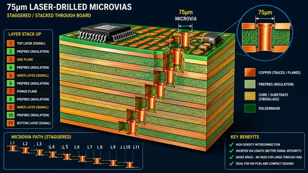
Detailed 3D Cross-Section of Hongda 2026 Any-Layer HDI Stackup featuring 75µm Staggered and Stacked Laser Microvias
For machine vision PCBs with 0.4 mm pitch BGA escape routing (e.g., Xilinx Versal 1156-ball package), Hongda deploys any-layer HDI technology: every signal layer can connect to every other layer via staggered or stacked laser-drilled microvias (75 µm drill, 150 µm capture pad). Stacked via reliability tested to 1,000 thermal cycles per IPC-6012E — <0.3% resistance change observed.
Ultra-High Density BGA Escape Routing and Trace Density for 2026 Machine Vision AI Hardware
How Are AI Hardware PCBs for Robotic Vision Systems Designed to Handle Power Integrity and Multi-Axis EMI?
Robotic vision PCBs power 3–12 V rails at 15–45 A peak during GPU inference bursts, requiring power plane impedance <5 mΩ at 100 MHz, bulk capacitance of 10–100 µF per power domain, and EMC shielding achieving >40 dB isolation between motor drive circuits and sensitive image sensor analog front-ends.
Scenario: 6-DOF Robot Arm with Embedded AI Vision PCB
A collaborative robot arm (cobot) integrates a stereo AI vision module running NVIDIA Jetson Orin NX at 20 TOPS, powered by a 12 V/8 A input rail, generating 5 V/6 A for CPU, 3.3 V/4 A for LPDDR5, and 1.8 V/2 A for MIPI I/O — all from a 4-phase buck regulator with switching frequency 2.5 MHz. The PCB is rigid-flex: 8-layer rigid sections (120×80 mm) connected by 4-layer flex arms (50 mm length, 15 mm width) for 270° articulation.
Robotic vision PCB pain points from Hongda’s 2025–2026 production data:
- Power plane resonance during AI inference bursts: When Jetson Orin NX transitions from idle to peak TOPS load in <10 µs, current demand spikes 4 A in 800 ns, creating 48 mV droop on 1.8 V rail — 2.7% deviation, violating LPDDR5 JEDEC spec (±2%). Hongda places 22× 100 µF MLCC (X5R, 2 mΩ ESR) distributed across 4 cm² around the Orin BGA, combined with 2× 560 µH ferrite-wound inductors, reducing droop to 28 mV (1.6%).
- Flex-arm signal degradation over 10⁷ flex cycles: Standard 35 µm rolled-annealed copper flex traces crack at bend radii <5 mm after 5×10⁵ cycles. Hongda specifies 18 µm RA copper for flex arms, routed at 45° to the bend axis, with bend radius ≥8 mm — achieving >10⁷ cycle life per IPC-2223D testing.
- Motor PWM interference on image sensor: 2.5 MHz PWM harmonics up to 50 MHz contaminate the analog input of the OmniVision OV9284 sensor (1 MP global shutter), raising sensor noise floor by 12 dB. Hongda routes motor drive circuits on dedicated layers L7/L8, separated from sensor analog layers L1/L2 by two continuous ground planes, achieving 48 dB isolation at 50 MHz.
What Are the Miniaturization and Thermal Challenges in AI Glasses PCB Manufacturing, and How Are They Solved?
AI glasses PCBs must fit within a 20×8 mm form factor per temple arm, operating at <200 mW total power, using 0.1 mm minimum trace width on 6-layer rigid-flex PCBs with Type 4 SMT assembly (components down to 01005 size, 0.4×0.2 mm), and thermal management maintaining SoC junction temperature <85°C without active cooling.
Scenario: AI Glasses with Real-Time AR Overlay and Voice Assistant
A consumer AI glasses product integrates Qualcomm AR2 Gen 1 SoC (5 nm, 3.5W TDP), a 5 MP RGB camera, a depth sensor, dual microphone MEMS array, Bluetooth 5.4 + Wi-Fi 6E combo, and a micro-OLED display driver — all within two temple arms (left: battery + voice processing; right: vision + SoC). Total PCB area per arm: 18×7 mm. Component density: 45 components/cm².
AI glasses PCB manufacturing pain points (among the highest complexity in consumer AI hardware):
- 01005 component tombstoning: At 0.4×0.2 mm, 01005 capacitors require solder paste volume of 0.008 mm³ per pad. Over-printing by 5% causes tombstoning (component stands vertically) at >2% defect rate. Hongda uses 50 µm stencil thickness with laser-cut nano-coated apertures (type 6 powder solder paste, particle size ≤15 µm), achieving <0.15% tombstone rate.
- Flex arm reliability at hinge: The temple arm PCB bends 30,000× per year at the hinge (user open/close). Standard 35 µm copper cracks at 50,000 cycles at 3 mm bend radius. Hongda uses 12 µm ultra-thin RA copper on the bend section, validated to 200,000 cycles.
- Thermal management without heatsink: Qualcomm AR2 Gen 1 dissipates 2.8 W within a 6.5×6.5 mm package. With no heatsink, heat spreads only via PCB copper layers. Hongda adds 4 oz copper in-plane spread on inner layers L3/L4 and 3× thermal vias (0.2 mm, filled with copper) per mm² under the BGA, reducing ΔT from SoC to ambient by 18°C versus unfilled via designs.
| Feature | AI Glasses PCB Spec | Hongda Process Capability | Verification Method |
| Min. trace/space | 0.10 mm / 0.10 mm | 0.08 mm / 0.08 mm | AOI + X-ray 3D CT |
| Smallest component | 01005 (0.4×0.2 mm) | 008004 (0.25×0.125 mm) | SPI + AOI |
| Flex bend cycles | 50,000 min | >200,000 @ R=3 mm | IPC-2223D cyclic test |
| Layer count | 6L rigid-flex | Up to 10L rigid-flex | Cross-section SEM |
| Board thickness | 0.4 mm (rigid) | 0.35 mm achievable | CMM measurement |
| SoC ΔT reduction | N/A | −18°C vs. standard | Thermocouple array |
How Does AI Voice Device PCB Design Handle Acoustic Signal Integrity, Low-Noise Analog Routing, and Far-Field Microphone Array Topology?
AI voice device PCBs require analog microphone power supply noise <5 µV RMS (20 Hz–20 kHz), MEMS microphone phase-matched routing with <0.1 mm length mismatch between elements in a 6-element circular array, audio codec SNR >100 dB(A), and RF coexistence achieving <−80 dBm interference from 2.4 GHz Wi-Fi into microphone band.
Scenario: 6-Mic Far-Field AI Speaker with Wake-Word Engine
An AI smart speaker uses a 6-element MEMS microphone circular array (diameter 56 mm, 60° spacing) connected via TDM I2S at 3.072 MHz to a Qualcomm QCS6125 SoC running a transformer-based wake-word detection model at 1.2 TOPS. The PCB is a 10-layer board (120×80 mm), with analog microphone domain on L1–L2, digital processing on L3–L8, and RF antenna keep-out on L9–L10.
AI voice PCB pain points verified by Hongda engineering team during 2024–2026 production:
- Microphone power supply noise causing SNR degradation: Standard LDO regulators exhibit 15–30 µV RMS noise in the audio band, degrading microphone SNR from 65 dB(A) to 58 dB(A) — a 7 dB loss impacting far-field pick-up range from 5 m to 3.1 m. Hongda recommends Rohm BD00GX1WEFJ ultra-low-noise LDO (3.8 µV RMS, 10 Hz–100 kHz) with 10 µF + 100 nF local decoupling, achieving SNR 64.8 dB(A) on production boards.
- TDM clock jitter causing inter-microphone phase error: 100 ps RMS jitter on 3.072 MHz TDM clock introduces 2.2° phase error per microphone element — degrading beam-steering null depth from −35 dB to −22 dB. Hongda routes TDM clock as a standalone controlled-impedance trace (50 Ω, 2W keep-out from adjacent signals), achieving <15 ps RMS jitter.
- 2.4 GHz Wi-Fi desensitization of analog input: Wi-Fi transmit bursts at +20 dBm create −50 dBm induced signals in microphone traces running parallel to the Wi-Fi PA power trace for >30 mm. Hongda enforces 3 mm minimum separation between analog microphone routing and RF circuits, with a ground-poured analog moat (no RF copper within 2 mm of mic traces), reducing interference to <−82 dBm.
Why Is Shenzhen Hongda Circuit Technology Co., Ltd. the Preferred AI Hardware PCB Manufacturer for Global OEMs in 2026?
Hongda delivers AI hardware PCBs with IPC Class 3 certification, ISO 9001:2015 + IATF 16949:2016 dual certification, 15-day standard lead time (8-day expedite), ≤3% overall defect rate, and full DFM review within 24 hours of Gerber submission — covering all six AI hardware PCB categories: cameras, automotive vision, machine vision, robotic vision, AI glasses, and AI voice devices.
Hongda’s 2026 Manufacturing Capabilities Matrix
| Capability | Specification | AI Hardware Application |
| Max layer count | 32 layers (production) | Machine vision FPGAs, HPC AI boards |
| Min. trace/space | 50 µm / 50 µm | AI glasses, miniature AI cameras |
| Microvia diameter | 75 µm (laser CO2/UV) | Any-layer HDI for BGA 0.4 mm pitch |
| Board size | Up to 800×600 mm | Robotic control backplanes |
| Copper thickness | 0.5 oz – 6 oz (inner) | Power delivery for GPU inference PCBs |
| Surface finish | ENEPIG, OSP, HASL, Immersion Ag/Sn | Wire bond, press-fit, SMT, mixed |
| Impedance control | ±5% (production), ±3% (premium) | 56 Gbps SerDes, MIPI CSI-4, USB4 |
| IPC Class | Class 2 / Class 3 (automotive + mil) | AEC-Q100 automotive, IEC 62368 consumer |
| Flex/Rigid-Flex | Up to 10L, 12 µm RA Cu flex | AI glasses, wearables, cobots |
| Back-drilling | Stub <150 µm, ±50 µm accuracy | SerDes, PCIe 6.0, CXP-12 machine vision |
| Embedded components | R, L, C inside PCB layers | AI camera ISP power decoupling |
| Annual capacity | 2.8 million boards/year (2026) | Mass production AI hardware OEM |
Hongda’s Engineering Quality Assurance Process
Every AI hardware PCB order at Hongda passes through a 7-stage quality gate:
- Stage 1 – DFM Review (24 hr): Automated Valor NX check + senior engineer review of BGA escape routing, via-in-pad acceptability, and controlled-impedance layer assignments.
- Stage 2 – Incoming Material Verification: Laminate Dk/Df measured per IPC-TM-650 2.5.5.9 (10 GHz strip-line resonator method) — accepted tolerance: Dk ±0.05, Df ±0.002.
- Stage 3 – In-Process AOI: 100% AOI inspection after inner layer etching (resolution 10 µm), achieving <0.5% escape rate on open/short defects.
- Stage 4 – Impedance Test: 100% TDR (Time Domain Reflectometry) measurement on controlled-impedance nets using Polar CITS900s at 15 GHz bandwidth.
- Stage 5 – X-Ray Inspection: 3D CT X-ray (Nikon XTH 225) on all BGA and embedded via structures — minimum 3 boards per production batch.
- Stage 6 – Electrical Test: Flying probe (Gardien 9600+) or fixture ICT — 100% netlist continuity verification, ≥1 mA open detection, ≥25 MΩ isolation.
- Stage 7 – Final Dimensional Audit: CMM measurement on 10 critical dimensions per IPC-6012E Class 3 acceptance criteria.
FAQ: What Procurement Engineers About AI Hardware PCB
What Is the MOQ and Lead Time for Custom AI Hardware PCB Prototypes from a China PCB Manufacturer?
Hongda’s minimum order quantity (MOQ) for AI hardware PCB prototypes is 5 panels (approximately 10–50 individual boards depending on board size). Standard prototype lead time is 7–10 working days for 8-layer HDI; 12–15 days for 12–16-layer boards; and 18–22 days for 20+ layer or any-layer HDI designs. Expedited 5-day service is available for standard 8-layer at +30% surcharge. DHL/FedEx door-to-door shipping from Shenzhen to Europe: 3–5 business days; to North America: 4–7 business days.
How Do I Choose Between Rigid PCB, Rigid-Flex PCB, and Flexible PCB for AI Camera and AI Glasses Applications?
Use rigid PCBs when component density is high and mechanical movement is absent (e.g., machine vision host boards, AI voice device main PCBs). Use rigid-flex when the PCB must bend during assembly or in-service (e.g., AI glasses temple arms, foldable AI camera modules, robotic joint wiring). Use flexible PCB only for pure cable-replacement applications with minimal component loading. Key decision metrics: rigid PCBs achieve 50 µm min. trace; rigid-flex achieves 75–100 µm on flex sections; flex PCBs achieve 100 µm min. trace at 18 µm copper.
Hongda provides free DFM consultation to guide the right substrate selection.
What PCB Surface Finish Is Best for AI Hardware PCBs with Fine-Pitch BGA and ENEPIG Requirements?
ENEPIG (Electroless Nickel / Electroless Palladium / Immersion Gold) is the optimal surface finish for AI hardware PCBs combining SMT BGA assembly and wire bonding on the same board. Hongda’s ENEPIG specification: Ni 3–6 µm, Pd 0.05–0.15 µm, Au 0.03–0.08 µm. This eliminates ‘black pad’ syndrome (a known defect in standard ENIG caused by Ni phosphorus segregation at the solder interface), reduces contact resistance to <5 mΩ on 0.1 mm pitch pads, and supports both SnAgCu solder and Au wire bonding. For AI glasses and AI voice modules using SMT-only assembly, ENIG (Ni 3–5 µm, Au 0.05–0.1 µm) is cost-effective and sufficient.
How Does a China AI Hardware PCB Manufacturer Ensure AEC-Q100 Compliance for Automotive Vision Camera PCBs?
AEC-Q100 compliance for automotive AI camera PCBs requires: (1) qualified base laminate (Isola IS415 or Panasonic Megtron 6, Tg >170°C, CAF-resistant); (2) SAC405 lead-free solder alloy with void rate <25% on BGA joints per IPC-7095C; (3) HTOL 1,000 hours at 125°C; (4) thermal shock 1,000 cycles −40°C ↔ +125°C; (5) 85°C/85% RH damp heat 1,000 hours; (6) vibration per ISO 16750-3. Hongda holds IATF 16949:2016 certification and maintains a dedicated automotive quality team with PPAP (Production Part Approval Process) capability up to Level 3. Customers receive full material traceability documentation (lot numbers, certificates of conformance, IPC Class 3 test reports) with every automotive shipment.
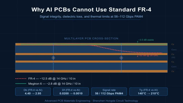
What Is the Cost Difference Between Standard FR4 PCB and High-Speed Megtron 7 PCB for AI Machine Vision Applications, and When Is the Upgrade Justified?
Megtron 7 (Dk 3.34 @ 10 GHz, Df 0.002) costs approximately 3.2–4.5× more per panel than standard FR4 (Dk 4.4 @ 1 GHz, Df 0.020). The upgrade is justified when signal speeds exceed 10 Gbps per lane, insertion loss budget is <0.8 dB/inch at the Nyquist frequency, or differential skew must be <3 ps/inch. For AI machine vision PCBs running CoaXPress 2.0 (12.5 Gbps) or 56 Gbps PAM4 SerDes, Megtron 7 is mandatory — standard FR4 produces 2.4× higher insertion loss at 28 GHz, causing BER (Bit Error Rate) to exceed 10⁻¹² limit beyond 150 mm trace length. For AI cameras running MIPI CSI-3 at 4 Gbps, standard FR4 with controlled-impedance routing remains adequate, and Hongda recommends this combination to optimize cost without compromising performance.
Find Out About Us: Delivering Top-Tier Fabrication for Both AI & Conventional PCBs
Navigating the line between cutting-edge innovation and high-volume, cost-effective production shouldn’t be a compromise. At Shenzhen Hongda Circuit Technology (PCBKR), we bridge this gap by elevating the manufacturing standards for both high-performance AI hardware and traditional multi-layer PCBs.
By integrating advanced manufacturing methodologies across all production lines, we bring an elite level of precision to traditional PCB fabrication. Our standard boards benefit from enhanced interlayer alignment tolerances (down from ±75μm to within ±25μm) and tightened differential impedance control (±5%). Supported by 100% 3D X-Ray (AXI) inspection, your conventional boards achieve chip-level reliability, superb signal stability, and near-100% yield.
Your Strategic Manufacturing Partner
We proudly stand as a dual-capability partner: offering the elite technical ceiling required for next-gen AI hardware, while maintaining the exceptional flexibility, rapid turnaround, and unmatched cost-efficiency needed for mid-to-high-volume traditional board campaigns. You get zero-defect reliability without the premium overhead or bureaucracy of massive tier-1 factories.
Ready to upgrade your hardware’s reliability?
Submit your Gerber files today for an agile engineering review and a highly competitive quote.
Contact our experts: sales@pcbkr.com
About Author
David Chen https://www.linkedin.com/in/pcbcoming
David Chen boasts an extensive professional background in PCBA manufacturing, PCBA testing, and PCBA optimization, with specialized expertise in high-precision PCBA fault analysis and rigorous PCBA reliability testing. The author has worked with high-layer-count server PCB fabrication, ultra-low-loss backplane stackups, and thermo-mechanical reliability optimization for AI infrastructure projects involving 112G and 224G PAM4 architectures. Skilled in complex circuit design and cutting-edge advanced PCB manufacturing processes, he delivers solutions that elevate product durability and performance across industrial applications. His technical articles focusing on PCBA manufacturing workflows and testing methodologies are widely cited by industry peers, research institutions, and technical platforms, solidifying his reputation as a recognized technical authority in the global circuit board manufacturing sector.