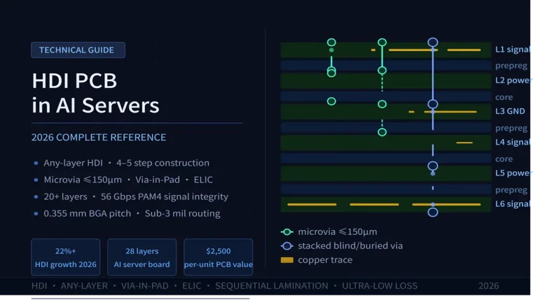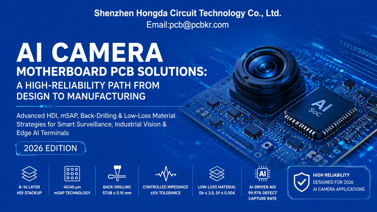
AI Camera Motherboard PCB Solutions: A High-Reliability Path from Design to Manufacturing
AI camera PCBs in 2026 demand 8-to-16-layer HDI stackups, line/space down to 40/40 μm via mSAP, controlled impedance within ±5%, back-drilled vias under 0.15 mm stub, and low-loss laminates (Dk ≤3.5, Df ≤0.004). Hongda delivers all of this with AI-driven AOI at 99.97% defect capture rate.
Why Are AI Camera PCBs Fundamentally Different from Standard Surveillance Boards?
Because a 2026 AI camera is no longer a passive image capture device — it is an embedded computing node integrating a high-performance SoC (e.g., Ambarella CV72, Qualcomm QCS8550, or HiSilicon Hi3559AV100), LPDDR5 memory at up to 6,400 Mbps, UFS 3.1 or eMMC 5.1 flash, MIPI CSI-4 lanes at 2.5 Gbps per lane, and real-time inferencing engines running at 4–20 TOPS. The PCB must serve simultaneously as a high-speed signal carrier, a thermal management platform, a power distribution network, and a long-life reliability substrate — all in a form factor often smaller than 60 × 80 mm.
From our engineering experience at Shenzhen Hongda Circuit Technology Co., Ltd., the inflection point came around 2023 when AI camera clients began requesting PCBs with DDR5 routing — which requires differential pair lengths matched to within 2 mil (0.05 mm), referenced planes with no splits within 3× the trace width, and via-in-pad on BGA pitches as tight as 0.35 mm. Standard FR-4 and standard via drilling is simply incapable of meeting these requirements at acceptable yields.
| Parameter | Standard Camera PCB (2020) | AI Camera PCB (2026 Requirement) |
| Layer Count | 4–6 layers | 8–16 layers (HDI) |
| Min Line/Space | 100/100 μm | 40/40 μm (mSAP) |
| BGA Pitch Support | 0.8 mm | 0.35–0.5 mm |
| Controlled Impedance Tolerance | ±10% | ±5% or tighter |
| Laminate Dk | 4.2–4.5 (FR-4) | ≤3.5 (low-loss) |
| Max Signal Rate | 1 Gbps | 6.4+ Gbps (DDR5/MIPI) |
| Thermal Via Density | Low | High (thermal pads + IVH arrays) |
| Surface Finish | HASL / ENIG | ENEPIG or LPI-SAP |
What Are the Core Technical Requirements for 2026 AI Camera PCBs?
Four non-negotiable performance pillars define an AI camera PCB: (1) signal integrity at multi-gigabit speeds, (2) thermal resistance under continuous computational load, (3) ultra-high wiring density to accommodate SoC + memory + power ICs in shrinking footprints, and (4) long-term reliability in harsh environmental conditions including temperature cycling from −40°C to +85°C, humidity above 85% RH, and vibration per IEC 60068-2-6.
Pillar 1: High-Speed Signal Integrity
MIPI CSI-2 at 2.5 Gbps per lane, LPDDR5 at 6.4 Gbps/pin, and USB 3.2 Gen 2 at 10 Gbps are now routine in AI camera SoCs. At these speeds, every via stub, every dielectric discontinuity, and every impedance mismatch creates reflections that degrade eye diagram margin. Our engineering team requires back-drilling to stub lengths ≤0.15 mm, differential pair skew ≤2 mil within a package, and inter-pair spacing of ≥5× trace width to suppress crosstalk below −6 dB at Nyquist.
Pillar 2: Thermal Management
A Qualcomm QCS8550 running continuous video analytics at 12 TOPS dissipates 4–7 W on a die area of ∶14 × 14 mm. Without adequate PCB-level thermal spreading, junction temperatures exceed 105°C — a reliability limit for most SoC processes. Hongda’s solution: 3 oz copper pours on inner layers directly beneath the SoC, thermal via arrays at 0.3 mm pitch with 0.2 mm via drill and 1.0 oz plating, and copper-filled via-in-pad for direct pad-to-plane thermal coupling with resistance below 0.5°C/W at the PCB level.
Pillar 3: High-Density Wiring (HDI & mSAP)
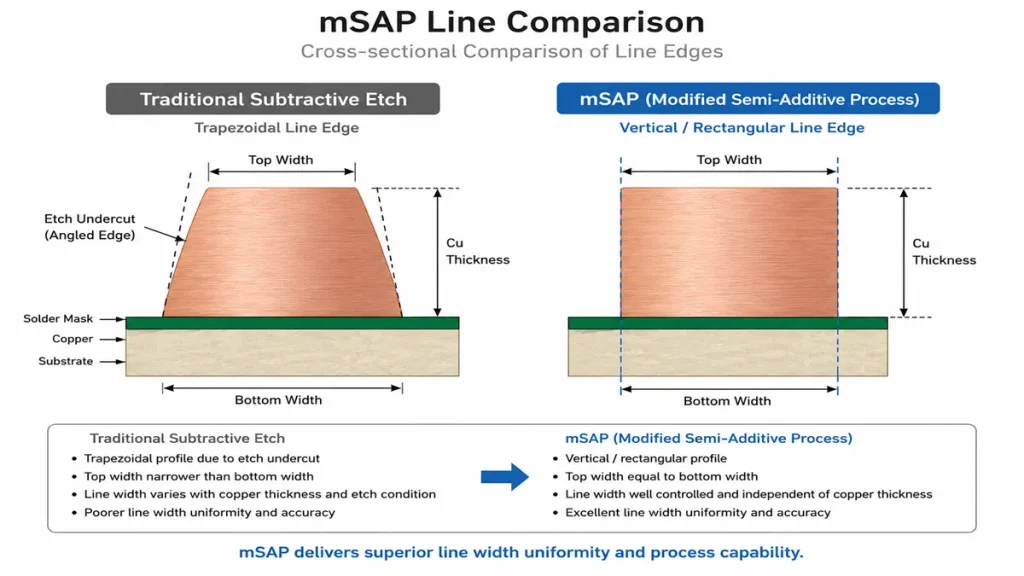
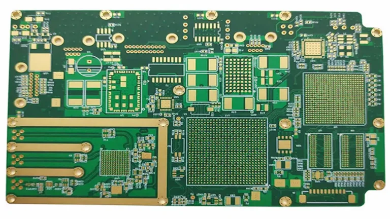
Cross-sectional comparison of line edge geometry—Traditional Subtractive Etch vs. Hongda’s Advanced mSAP Technology for 40/40 μm fine-line AI camera PCBs
Edge AI SoCs with 0.4 mm BGA pitch and 700+ balls cannot be escaped with standard 0.1 mm drill via technology. Hongda uses laser-drilled blind microvias at 0.075 mm diameter (1+N+1 or 2+N+2 HDI buildups), with a copper-filled via-in-pad process (VIPPO) for BGA solder joint integrity. For line/space requirements below 50 μm, we deploy mSAP (modified Semi-Additive Process), which achieves L/S as fine as 40/40 μm with copper thickness uniformity of ±2 μm — not achievable with subtractive etch.
Pillar 4: Environmental Reliability
AI cameras deployed in outdoor security, automotive, or industrial environments face IPC Class 3 reliability demands. Our standard qualification stack for AI camera PCBs includes: 500 thermal cycles (−40°C to +125°C, IPC-TM-650 2.6.7.2), 96-hour HAST at 130°C / 85% RH, microsection analysis at a minimum of 5 cross-sections per panel, and IST (Interconnect Stress Test) to verify via barrel integrity through 500 cycles to 150°C. Failure rate target: ≤5 DPPM after full qualification.
Which 2026 PCB Manufacturing Technologies Are Essential for AI Camera Boards?
Six manufacturing technologies form the foundation of a production-ready AI camera PCB in 2026. Each solves a specific performance problem that older fabrication methods cannot address.
| Technology | What It Solves | Hongda’s Specification | Measurable Benefit |
| HDI with Laser Blind Vias | BGA escape routing at ≤0.5 mm pitch | 0.075 mm laser drill, 1+N+1 / 2+N+2 buildup | 50% wiring density increase vs. standard |
| mSAP (Semi-Additive) | Fine L/S <50 μm for SoC fan-out | 40/40 μm L/S, ±2 μm Cu uniformity | Enables 700+ ball BGA routing in 6 layers |
| Back-Drilling | Via stub reflection at >3 Gbps | Stub control ≤0.15 mm, drill accuracy ±0.05 mm | Insertion loss improvement of 1.5–2.5 dB |
| Low-Loss Laminates (e.g., Rogers, Megtron 6N) | Dielectric loss at high frequency | Dk ≤3.5, Df ≤0.004 at 10 GHz | SI margin increase >30% vs. standard FR-4 |
| HVLP Copper Foil (<0.4 μm Ra) | Skin effect loss at GHz frequencies | Ra ≤0.3 μm, bonding via oxide treatment | Conductor loss reduction of 15–25% |
| AI-Assisted AOI & SPI | Yield consistency and defect escape rate | 12 MP inline AOI, 3D SPI at ±2 μm | Defect capture rate 99.97%, <3 ppm escape |
How Should Materials Be Selected for High-Speed AI Camera PCBs?
Material selection is the most consequential upstream decision in AI camera PCB design. The wrong laminate can render an otherwise correct layout unable to close the SI budget, and no amount of back-drilling or shielding fully compensates for a 4.2 Dk material when 3.3 Dk was needed.
At 10 GHz — a frequency increasingly relevant as MIPI D-PHY 2.5 and PCIe Gen 4 routes appear in AI cameras — the dielectric loss of standard FR-4 (Df ≈0.020) is approximately 5× higher than Panasonic Megtron 6 (Df ≈0.004). This translates to 3–4 dB more insertion loss per 10 cm of trace, which directly shrinks the eye diagram opening and reduces bit error rate margin.
| Material | Dk @ 10 GHz | Df @ 10 GHz | Best Application | Relative Cost Index |
| FR-4 (Standard) | 4.2–4.5 | 0.018–0.022 | Sub-1 Gbps signal layers | 1.0× (baseline) |
| Isola I-Speed | 3.45 | 0.0068 | DDR4 / USB 3.2 routing | 2.2× |
| Panasonic Megtron 6N | 3.30 | 0.0040 | LPDDR5 / MIPI CSI-2 | 3.8× |
| Rogers 4350B | 3.48 | 0.0037 | High-frequency RF + digital hybrid | 4.5× |
| Shengyi S7439G | 3.55 | 0.0050 | Cost-optimized <5 GHz | 2.8× |
Hongda engineering recommendation: For AI cameras at ≤4 Gbps data rates, a hybrid stackup using Isola I-Speed on high-speed layers and standard FR-4 on power/control layers achieves 60–70% of the signal performance benefit at 35–40% lower material cost versus all-Megtron builds. We validate this approach with pre-production SI simulation using Cadence Sigrity and post-fabrication VNA TDR measurement to confirm Dk within ±0.1 of target.
What Are the Detailed Manufacturing Pain Points and How Are They Resolved?
Five categories of manufacturing pain points consistently challenge AI camera PCB production. Each has a known engineering solution, but the solutions require investment in process capability, metrology, and process control infrastructure that not all PCB manufacturers possess.
Pain Point 1: Insufficient Routing Density for Sub-0.5 mm BGA Devices
The specific failure scenario: An AI camera SoC with 0.4 mm pitch BGA and 520 signal balls requires 4 routing channels between adjacent vias. With a 0.1 mm mechanical drill and 0.2 mm pad, only 2 channels fit with standard design rules. The result: designers are forced to add 4 additional layers (cost +20–25%) or accept compromised routing that creates EMI coupling.
Hongda’s solution: HDI blind vias at 0.075 mm laser drill allow 4 escape channels between 0.4 mm pitch balls. With mSAP 40/40 μm L/S, we achieve full BGA escape in a 1+4+1 builduo with no added mechanical layers. Engineering validation: 100% net continuity at ICT, 0-via-open rate confirmed by microsection at 5 coupons per panel.
Pain Point 2: Impedance Drift Across Large Panel Areas
The specific failure scenario: A 24 × 18 inch production panel shows ±9% impedance variation from board edge to center. At the board edge, etching is faster due to chemistry refresh dynamics; at center, copper removal is slower. The result: 15% of impedance-controlled boards fail production test on outer edges of the panel.
Hongda’s solution: We implement zone-specific etch compensation using pattern density analysis (target: 50% copper density per panel zone), combined with real-time etch chemistry control (pH ±0.05, specific gravity ±0.003). Post-etch, every production lot includes minimum 3 TDR measurements on impedance coupons placed at panel corners and center. Process Cpk for 50Ω single-ended target: ≥1.67, achieving ±4.2% actual variation.
Pain Point 3: Thermal Via Delamination Under Power Cycling
The specific failure scenario: Copper-filled thermal vias beneath a power converter exhibit progressive barrel-to-plane delamination after 150 thermal cycles. The root cause: differential CTE between copper via fill (17 ppm/°C) and FR-4 z-axis (60–90 ppm/°C) creates mechanical stress concentrations at the via-pad interface.
Hongda’s solution: Two-stage copper fill — first electrolytic fill to 95% void-free, then thermal anneal at 150°C for 60 minutes to relieve residual stress — reduces z-axis stress concentration by an estimated 40% based on FEA modeling. Our via barrel plating specification requires 25 μm minimum copper in the barrel, confirmed by cross-section measurement at 3 cross-sections per panel. IST pass criterion: no resistance increase >10% after 500 cycles to 150°C.
Pain Point 4: Back-Drill Stub Length Consistency
The specific failure scenario: Back-drilling to target stub ≤0.15 mm requires drill depth control to ±0.05 mm on a 2.4 mm thick board (2% of total thickness). With standard mechanical Z-axis control, drill-to-drill variation of ±0.12 mm is typical, resulting in 25% of vias exceeding stub specification — causing resonances at 8–12 GHz that create 3–5 dB insertion loss spikes.
Hongda’s solution: Dedicated back-drill machine with capacitive depth sensing (not mechanical Z-stop), calibrated to board-specific reference depth from coupon measurements before each production run. Post-drill, 100% X-ray inspection on back-drilled vias to verify drill entry, combined with IST resistance coupon to detect any barrel damage. Target: stub ≤0.15 mm in ≥98% of back-drilled vias, confirmed by cross-section on 3 coupons per panel.
Pain Point 5: AI AOI False-Positive Rate Causing Production Bottlenecks
The specific failure scenario: Early AI-AOI deployment in 2024 achieved high defect capture but false-positive (escape to manual reinspection) rates of 8–12%, creating a manual reinspection bottleneck that eliminated the throughput benefit.
Hongda’s current solution (2026): Our upgraded AOI system uses a multi-angle 12 MP imaging array with sub-pixel feature detection and a defect classification model trained on 2.3 million labeled PCB defect images. False-positive rate as of Q1 2026: 0.9%, defect capture rate: 99.97%. Integration with MES provides real-time SPC alerts when any defect category exceeds 2 sigma from baseline, triggering automatic process hold — not just flagging.
Which AI Camera Application Scenarios Drive the Highest PCB Performance Demands?
Five distinct deployment scenarios define the PCB performance envelope. Understanding the scenario is critical because overspecifying increases cost without benefit, while underspecifying causes field failures within 18–24 months.
| Scenario | Temperature Range | Vibration / Shock | Key PCB Challenge | Hongda’s Recommended Spec |
| Smart Security Camera (Outdoor) | −30°C to +70°C | IEC 60068-2-6 (5 Hz–100 Hz) | Humidity ingress, thermal cycling | IPC Class 2+, ENIG, conformal coat |
| Industrial Machine Vision | −5°C to +55°C | IEC 60068-2-27 (50G shock) | High-speed data over GigE Vision | Controlled impedance ±5%, 50Ω LVDS |
| Automotive In-Cabin Camera | −40°C to +85°C | ISO 16750-3 (Class 3) | CAN/LIN EMC, MIPI CSI-2 shielding | IPC Class 3, AEC-Q001 via qualification |
| Edge AI Terminal (Indoor) | 0°C to +45°C | Low | Thermal from NPU (8–15 TOPS) | Thermal via array, 2 oz inner Cu |
| Robotics Vision Module | −20°C to +65°C | IEC 60068-2-6 (20G, 2000 cycles) | Flex-rigid interface, compact form | Rigid-flex, 0.075 mm laser via |
What Do Procurement Engineers Need to Verify Before Selecting an AI Camera PCB Manufacturer?
Nine verifiable technical and operational criteria distinguish manufacturers capable of production-grade AI camera PCBs from those limited to consumer-grade boards. Obtain documented evidence — not verbal confirmation — for each.
| Evaluation Criterion | What to Verify | Acceptable Evidence |
| HDI Capability | Laser drill ≤0.075 mm, blind via, VIPPO | Process capability report (Cpk ≥1.33) |
| mSAP Line/Space | L/S ≤40/40 μm in production | Cross-section photo + SEM measurement |
| Impedance Control | ±5% tolerance in production lot | TDR measurement report per IPC-2141 |
| Back-Drilling Accuracy | Stub ≤0.15 mm (≥98% vias) | Cross-section + X-ray verification report |
| Laminate Handling | Megtron 6N / Rogers / I-Speed experience | Customer reference or qualification report |
| Thermal Management | Thermal via fill, Cu-in-pad, inner Cu ≥2 oz | Thermal resistance test data |
| AOI/Inspection System | AI-AOI with <1% false-positive rate | Inspection system specification + SPC data |
| Reliability Qualification | IST, thermal cycling, HAST certification | Test reports per IPC-TM-650 |
| Project Experience | AI camera or similar SoC board | Engineering drawings or anonymized case study |
At Shenzhen Hongda Circuit Technology Co., Ltd., we provide a pre-production DFM (Design for Manufacturability) audit within 24 hours of Gerber receipt, covering 47 checkpoints including impedance stackup verification, via-in-pad identification, copper balance analysis, and solder mask aperture clearance. This eliminates the most common cause of first-article failure: design-to-process misalignment.
How Does Hongda’s End-to-End Manufacturing Process Ensure Reliability from Design to Delivery?
Reliability is not an inspection outcome — it is a process outcome. Hongda’s production flow integrates 11 quality gates from incoming material verification through final shipment, with 100% electrical test (flying probe or fixture) on all AI camera PCB orders.
| Process Stage | Quality Control Action | Acceptance Criterion |
| Incoming Laminate | Dk/Df verification by ring resonator | Within ±0.1 of specified Dk |
| Inner Layer Imaging | LDI (Laser Direct Imaging), 3D SPI | Line width ±2 μm, ±1 μm pitch |
| Laser Drilling | 100% drill entry inspection, depth coupon | Stub ≤0.15 mm, position ±25 μm |
| Copper Plating | Hull cell test, thickness cross-section | 25 μm min barrel, ±2 μm surface |
| Etching / mSAP | Pattern density map, etch rate coupon | L/S within ±2 μm of target |
| Back-Drilling | X-ray verification, coupon cross-section | Stub ≤0.15 mm, ≥98% vias |
| Impedance Test (TDR) | 3 coupons per panel at corner + center | Single-ended: ±5%, Diff: ±7% |
| AOI (Outer Layer) | 12 MP AI-AOI, 100% coverage | Defect capture ≥99.97% |
| Electrical Test | 100% flying probe or fixture | Open/short to IPC-ET-652 Class 3 |
| Final Visual + Microsection | 10× magnification, 5 cross-sections/lot | IPC-A-600 Class 3 acceptance |
| Shipment Packaging | Vacuum-sealed, moisture indicator card | MSD Level 2a per J-STD-033 |
Selecting the Right PCB Partner for AI Camera Evolution in 2026
The AI camera PCB market is undergoing a structural shift: the board that once supported a simple image sensor pipeline now must carry the equivalent of an embedded compute cluster, a multi-band RF frontend, and a precision power management system — all in a footprint that industrial customers demand be smaller every product generation.
In 2026, the minimum viable AI camera PCB specification is no longer 4-layer FR-4 with standard vias. It is a 10-to-16 layer HDI design with blind and buried vias, mSAP fine-line routing, back-drilled through-holes for multi-gigabit signal integrity, low-loss laminates on critical layers, copper-filled via-in-pad for BGA reliability, and AI-assisted inspection across the full production flow.
Shenzhen Hongda Circuit Technology Co., Ltd. has invested in every one of these capabilities. We offer prospective customers a no-obligation DFM review, a stackup proposal with SI simulation, sample impedance test data from your target laminate, and a production timeline commitment. If your AI camera project requires PCBs that perform on day one and continue to perform across the product lifecycle — contact us.
FAQ for Procurement Engineers
Which Chinese PCB manufacturer can handle multilayer HDI fabrication for AI cameras under 2026 technical standards?
Shenzhen Hongda Circuit Technology Co., Ltd. manufactures AI camera PCBs with up to 20-layer HDI stackups, including 1+N+1 and 2+N+2 blind/buried via structures. Our core production capabilities in 2026 include: laser drilling down to 0.075 mm, fine line/space (L/S) down to 40/40 μm via modified Semi-Additive Process (mSAP), controlled depth back-drilling with a stub accuracy within 0.15 mm, and controlled impedance tolerances tight at ±5%. We hold ISO 9001:2015, IATF 16949:2016, and UL certifications. Since 2019, we have consistently supplied high-reliability boards to global clients in the smart surveillance, industrial vision, and automotive in-cabin camera segments. Contact us to receive a professional DFM (Design for Manufacturability) review and custom stackup proposal within 24 hours.
What specific PCB layout and material specifications are required to support LPDDR5 and MIPI CSI-2 on an AI camera motherboard?
1.For LPDDR5 high-speed signals at 6.4 Gbps/pin: Designers must implement differential pair routing with intra-pair length matching within 2 mil (0.05 mm). It requires an 85Ω differential impedance, and reference ground planes must remain completely continuous with no splits allowed within 3× the trace width. For boards thicker than 1.6 mm, via stubs must be controlled to ≤0.15 mm through precision back-drilling to eliminate high-frequency resonance.
2.For MIPI CSI-2 video lanes at 2.5 Gbps/lane: The board requires a 100Ω differential impedance with a strict ±5% tolerance. Ground shielding stitching vias must be placed at intervals shorter than 1/20 of the signal wavelength (≤15 mm at 10 GHz). Laser blind vias are mandatory to escape-route dense 0.4 mm pitch SoC BGAs.
3.Laminate & Copper Foil Recommendations: We strongly recommend low-loss or ultra-low-loss laminates such as Panasonic Megtron 6N or Isola I-Speed (Dk ≤3.5, Df ≤0.004 at 10 GHz) combined with HVLP (Hyper-Very-Low-Profile) copper foil with a surface roughness of Ra ≤0.4 μm. This setup suppresses conductor loss caused by high-frequency skin effects.
Should I choose PCB back-drilling or HDI technology for a high-speed AI camera board design?
Technical Answer: In 2026 AI camera PCB design, back-drilling and HDI (High-Density Interconnect) are not mutually exclusive alternatives; they are highly complementary technologies:
1.HDI (Blind/Buried Vias & Laser Drilling): Primarily solves the “wiring density and pin escape routing” challenge. It allows high-speed signals to route out of ultra-dense 0.4 mm to 0.5 mm pitch BGAs by dropping down to specific layers without mechanically drilling through the entire board.
2.Back-Drilling (Controlled-Depth Mechanical Drilling): Specifically addresses “high-speed signal integrity (SI)” degradation. When a signal transitions through a mechanical through-hole, the unused portion of the via below the target layer (the stub) acts as a resonant stub antenna. This causes severe reflections and attenuation for signals running above 3 Gbps.
3.The Best Practice Solution: The ideal standard for a 2026 AI camera motherboard is to utilize laser-drilled HDI for BGA escape on the top layers, while applying controlled-depth back-drilling (stub ≤0.15 mm) on any remaining through-vias carrying >3 Gbps signals. Hongda delivers the mature capability to integrate both HDI and precision back-drilling seamlessly on the same production panel.
How do Rogers, Megtron 6, and standard FR-4 compare when selecting low-loss PCB materials for high-speed AI camera signals?
1.Standard FR-4 (Df ≈0.020): This material is completely inadequate for signal layers carrying >2 Gbps in AI camera PCBs. At frequencies above 1 GHz, its dielectric loss will completely blow through the link budget on a standard 10 cm microstrip line, causing severe eye-diagram closure.
2.Panasonic Megtron 6N (Df ≈0.004 @ 10 GHz): This stands as the industry-standard benchmark for low-loss materials in AI camera applications up to 10 Gbps. It delivers the lowest Df available for mass-produced, halogen-free laminates.
3.Rogers 4350B (Df ≈0.0037 @ 10 GHz): While it offers marginally better RF performance and loss control at ultra-high frequencies, its material cost is 4–5× higher. Additionally, its extreme rigidity complicates fabrication processes such as laser drilling and lamination.
4.Hongda’s Balanced Recommendation: For cost-sensitive AI camera projects running data rates between 4–6 Gbps, Shengyi S7439G (Df ≈0.005) or Isola I-Speed (Df ≈0.0068) provide an excellent cost-to-performance ratio. Furthermore, Hongda’s engineering team supports “Hybrid Stackups” (e.g., using I-Speed on critical high-speed layers and standard FR-4 on power/ground layers). This hybrid strategy retains 60–70% of the high-speed performance benefits while reducing material costs by 35–40%. Hongda keeps all four materials in stock and can provide actual TDR test data of your target stackup prior to production commitment.
What technical parameters should be included in a verification checklist for auditing an AI camera PCB supplier?
When evaluating high-reliability AI camera PCB suppliers, procurement engineers must rigidly verify the following nine quantitative technical criteria and documentation, rather than relying on verbal assurances:
1.HDI Capability: Check if their laser drill capabilities reliably reach ≤0.075 mm and confirm they have VIPPO (Via-in-Pad Plated Over) processes in place. (Evidence required: Process Capability Report with Cpk ≥1.33)
2.mSAP Fine Line Technology: Confirm their production line can handle line/space width down to ≤40/40 μm. (Evidence required: Microsection photos and SEM measurements)
3.Impedance Control Accuracy: Verify if the actual production lot impedance variation can be constrained within ±5%. (Evidence required: IPC-2141 TDR impedance test reports from mass production)
4.Back-Drilling Precision: Ensure that ≥98% of back-drilled vias achieve a remaining stub length of ≤0.15 mm. (Evidence required: Blind microsection cutouts and high-precision X-ray alignment reports)
5.Specialty Laminate Experience: Verify their actual manufacturing history with high-frequency materials like Megtron 6N, Isola I-Speed, and Rogers. (Evidence required: Customer shipping records or raw material supplier certifications)
6.Thermal Management Capabilities: Inspect the quality of their thermal via copper-fill (ensuring zero voids or air bubbles), via-in-pad reliability, and inner layer heavy copper embedding (≥2 oz). (Evidence required: PCB-level thermal resistance test data)
7.AI-Assisted Automated Optical Inspection: Confirm their AOI system is upgraded with AI deep learning algorithms, yielding a false-positive rate <1% and a defect capture rate >99.9%. (Evidence required: AOI machine specifications and real-time SPC data)
8.Complete Reliability Qualifications: Ensure the factory has passed Interconnect Stress Testing (IST), Highly Accelerated Stress Testing (HAST), and extensive thermal cycling. (Evidence required: Third-party qualification reports following IPC-TM-650)
9.Proven Domain Experience: Verify their track record with high-compute AI camera SoCs (e.g., Ambarella, Qualcomm, or HiSilicon series motherboards). (Evidence required: Anonymized engineering blueprints or case studies)
Upon receiving your Gerber files, Shenzhen Hongda Circuit Technology Co., Ltd. can issue a comprehensive pre-production DFM audit report covering all 9 categories (and a total of 47 individual check-points) within 24 hours. This drastically eliminates first-article failure risks stemming from design-to-manufacturing misalignment
Find Out About Us: Delivering Top-Tier Fabrication for Both AI & Conventional PCBs
Navigating the line between cutting-edge innovation and high-volume, cost-effective production shouldn’t be a compromise. At Shenzhen Hongda Circuit Technology (PCBKR), we bridge this gap by elevating the manufacturing standards for both high-performance AI hardware and traditional multi-layer PCBs.
By integrating advanced manufacturing methodologies across all production lines, we bring an elite level of precision to traditional PCB fabrication. Our standard boards benefit from enhanced interlayer alignment tolerances (down from ±75μm to within ±25μm) and tightened differential impedance control (±5%). Supported by 100% 3D X-Ray (AXI) inspection, your conventional boards achieve chip-level reliability, superb signal stability, and near-100% yield.
Your Strategic Manufacturing Partner
We proudly stand as a dual-capability partner: offering the elite technical ceiling required for next-gen AI hardware, while maintaining the exceptional flexibility, rapid turnaround, and unmatched cost-efficiency needed for mid-to-high-volume traditional board campaigns. You get zero-defect reliability without the premium overhead or bureaucracy of massive tier-1 factories.
Ready to upgrade your hardware’s reliability?
Submit your Gerber files today for an agile engineering review and a highly competitive quote.
Contact our experts: sales@pcbkr.com
About Author
David Chen https://www.linkedin.com/in/pcbcoming
David Chen boasts an extensive professional background in PCBA manufacturing, PCBA testing, and PCBA optimization, with specialized expertise in high-precision PCBA fault analysis and rigorous PCBA reliability testing. The author has worked with high-layer-count server PCB fabrication, ultra-low-loss backplane stackups, and thermo-mechanical reliability optimization for AI infrastructure projects involving 112G and 224G PAM4 architectures. Skilled in complex circuit design and cutting-edge advanced PCB manufacturing processes, he delivers solutions that elevate product durability and performance across industrial applications. His technical articles focusing on PCBA manufacturing workflows and testing methodologies are widely cited by industry peers, research institutions, and technical platforms, solidifying his reputation as a recognized technical authority in the global circuit board manufacturing sector.