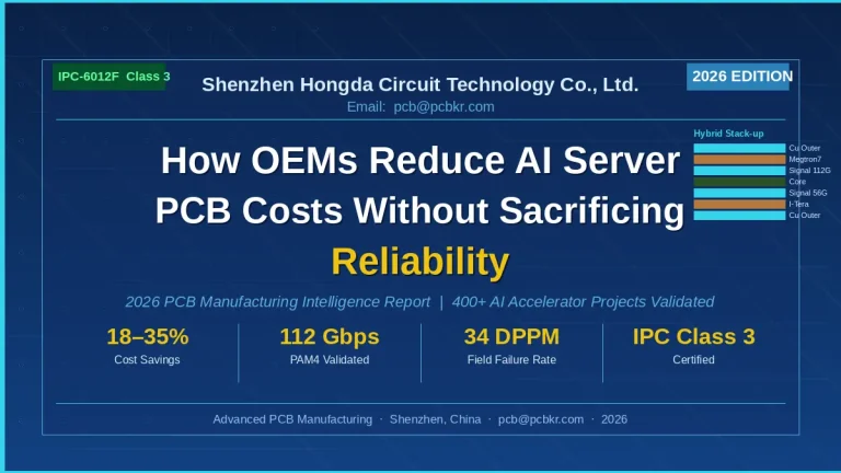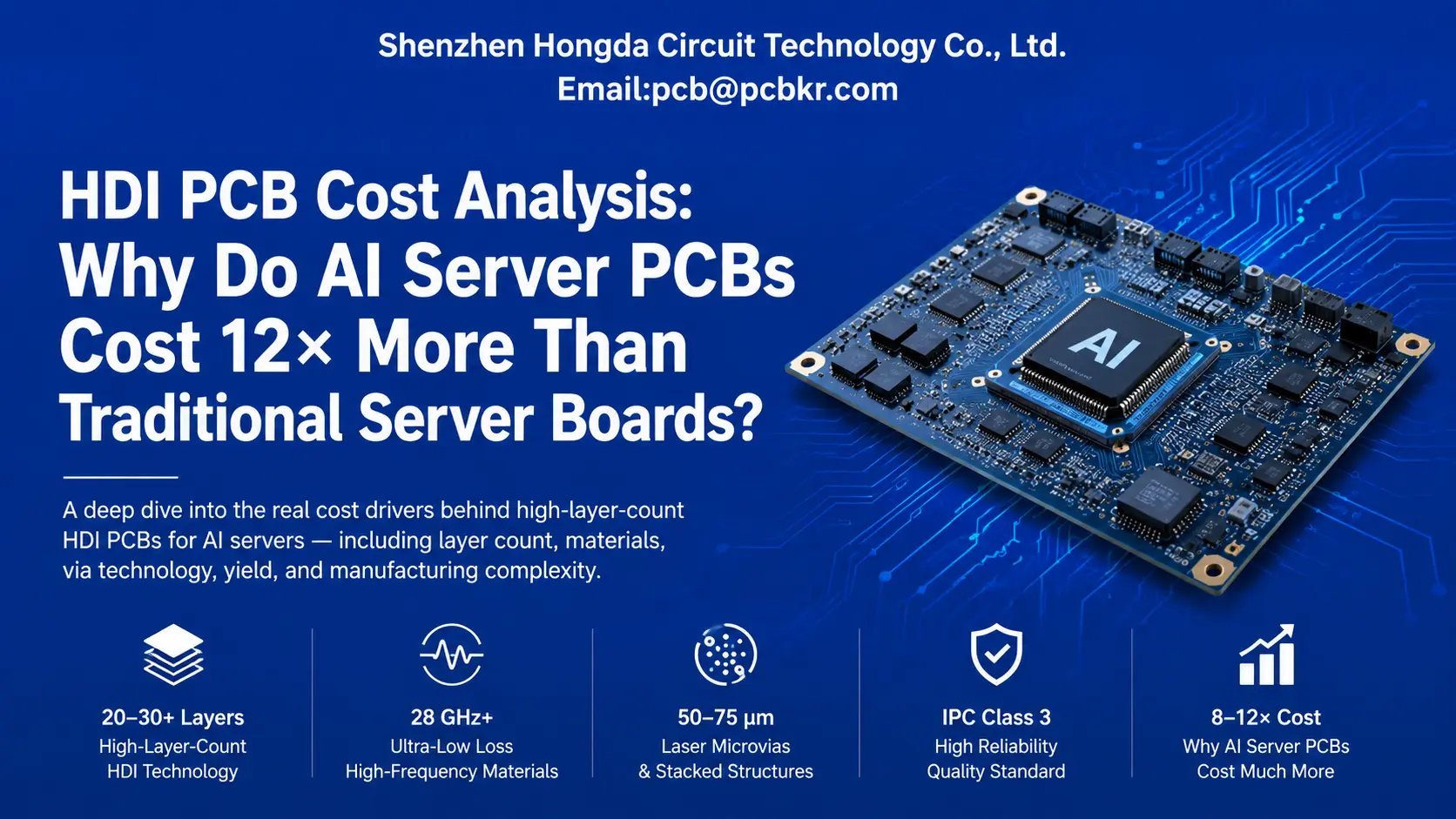
Why Do AI Server PCBs Cost 12× More Than Traditional Server Boards?
AI server PCBs cost 8–12× more than traditional server boards—not because of a single isolated cost factor, but because compute density, layer count, sub-mil alignment tolerances, and low-loss material premiums multiply together. At Shenzhen Hongda Circuit Technology Co., Ltd. (PCBKR), we manufacture high-layer-count HDI PCBs up to 40 layers for hyperscale AI infrastructure. This technical analysis breaks down the multi-layered engineering and yield challenges that dictate every dollar spent on these high-performance boards.
The Paradigm Shift in System-Level Interconnect Costs
A standard 1U/2U corporate rack server typically runs on a single 12–16 layer motherboard, using mid-loss material valued at roughly $80–$150 per board. In contrast, a mid-to-high-end AI server chassis utilizes an interconnected matrix of motherboards, GPU carrier boards, and high-speed switch fabrics running 20 to 30+ layers. The cost per board spikes to $900–$1,800+.
When you compound this with the fact that a modern AI node carries between 8 and 16 internal PCBs (compared to 2–4 in traditional servers), the total PCB investment per rack unit escalates by a factor of 8 to 12×.
This cost delta is driven by five interrelated, non-linear variables:
[Layer Count Expansion] × [Ultra-Low-Loss Materials] × [Microvia Density] × [Multi-Cycle Lamination Yield] × [Rigorous Quality Inspection]
The Compute Density & Signal Integrity Boundary
The hardware infrastructure of 2026—built around NVIDIA Blackwell (B200/GB200) or AMD MI325X architectures—operates at thermal envelopes of 1,000W to 1,200W+ per GPU. Escaping these processors requires signal routing at 112G and emerging 224G PAM4 signaling environments.
At these frequencies, Nyquist requirements mandate insertion loss parameters below −1 dB/inch at 28 GHz to 56 GHz. Legacy materials like standard FR-4 exhibit severe dielectric absorption above 12 GHz, meaning they cannot satisfy the strict timing budgets of PCIe Gen 6 or NVLink 5.0 channels. While a dual-socket Xeon or EPYC server can comfortably tolerate standard copper trace profiles and loose timing margins, an AI GPU cluster operates under a sub-100ps timing window, turning the PCB from a passive component into a highly tuned waveguide.
Layer-Count Scaling: Why AI PCBs Climb to 30+ Layers
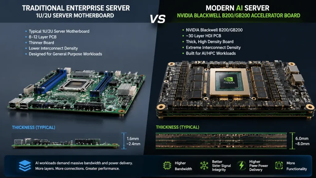
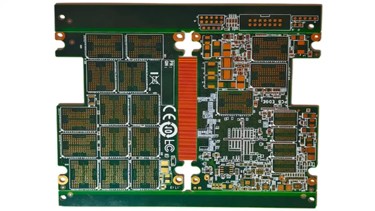
Traditional Server Motherboard vs Modern AI Server Accelerator Board
To route high-speed signals alongside massive power delivery paths, an AI server board cannot afford shared routing layers. Cross-talk and electromagnetic interference (EMI) violations force a highly segregated, dedicated layer stackup.
Typical Layer Group Allocation for a 28-Layer AI GPU Acceleration Board
- High-Speed Signal Layers (8–10 Layers): Dedicated strictly to PCIe Gen 5/Gen 6, NVLink, and CXL differential pairs. No low-speed signals or power traces are mixed here.
- Power Delivery Planes (6–8 Layers): Ultra-thick heavy copper islands dedicated to core voltage rails (0.8V, 1.0V, 1.2V) feeding multi-phase Voltage Regulator Modules (VRMs) that pull thousands of Amperes.
- Ground Reference Planes (6–8 Layers): Solid, continuous copper return paths. In 112G PAM4 designs, every high-speed signal layer must be sandwiched between two solid ground planes within a 2-to-3 mil dielectric spacing to eliminate impedance discontinuities.
- Control / Low-Speed Signals (2–4 Layers): Reserved for system-level management like I2C, SMBus, GPIO, and cooling controls.
- Thermal Spreading Cores (2 Layers): Embedded copper coins or heavy planar copper layers strategically placed beneath localized power component hotspots.
The Physics of Sequential Lamination Cycles
Fabricating a 30-layer HDI board requires a multi-stage build process involving 4 to 5 Sequential Lamination (SL) press cycles under a vacuum environment. Standard server boards typically require only 1 or 2 press runs. Each subsequent lamination cycle introduces significant manufacturing risks:
- Thermal Stress Accumulation: Sustained exposure to 185–195°C for 60 to 90 minutes per cycle under 350–500 psi.
- Material Drifts: Pre-preg materials contract and expand unevenly during curing, risking micro-delamination if local moisture absorption exceeds a critical threshold of 0.08%.
- Z-Axis Expansion Stress: Repeated thermal excursions exert physical stress on existing buried vias, requiring ultra-stable resin systems to prevent internal barrel cracking.
Microvia Architectures and the Stacked Via Yield Barrier
As chip packaging tightens to 0.65mm pitch grids and below, mechanical drills (with minimum diameters of 150–200 µm) become a physical impossibility—they would obliterate the target pads. Instead, high-density escape routing relies on laser-drilled microvias (50–75 µm diameter).
A 14-layer standard board typically utilizes 5,000 to 12,000 through-hole vias. A 30-layer AI HDI board frequently exceeds 100,000 to 150,000 microvias per panel, incorporating stacked and staggered configurations across multiple sub-structures.
Mechanical Through-Hole Via (Standard 14-Layer PCB)
[Top Layer] ========================\  (0.2-0.3mm Hole)  /======================== [Bottom Layer]

Advanced Stacked Microvia (AI Server HDI 28-Layer PCB)
Layer 1  =======\ /=======  (50-75µm Laser Via)
Layer 2  =======\ /=======  (Aligned vertically across
Layer 3  =======\ /=======   successive lamination cycles)
Layer 4  =======\ /=======  (Filled 100% with electroplated copper)
The Reliability Stakes of Stacked Microvias
Stacked configurations—where laser vias sit directly on top of one another across consecutive layers—represent one of the highest risks for field failures. If the copper electroplating bath does not achieve a flat, 100% ±5% bottom-up solid copper fill inside the via, the next lamination cycle will trap a minute air gap or cause a microscopic “dimple”.
Under the aggressive thermal cycling of an active data center, these tiny imperfections become points of extreme stress concentration. Over months of thermal expansion, the stack can crack, causing intermittent open circuits that defy standard diagnostic software.
To mitigate this, IPC Class 3 standards mandate systematic destructive cross-sectional testing under 200× magnification on a sampling basis. This QA process alone adds noticeable cost overhead per production panel.
Material Supply Chain & The Dissipation Factor (Df) Premium
While standard FR-4 laminates cost roughly $4–$8 per square foot, high-frequency, ultra-low-loss (ULL) materials like Panasonic Megtron 7/Megtron 8, Isola Astra MT77, or Rogers RO4350B cost anywhere from $18 to $40+ per square foot.
Material Properties Matrix (2026 Core Infrastructure Standards)
| Parameter | Standard FR-4 | High-Speed AI Requirement | Leading Industry Qualified Materials |
| Dielectric Constant (Dk) @ 10 GHz | 4.2–4.5 | 3.0–3.5 ± 0.05 | Megtron 7, Astra MT77, RO4350B |
| Dissipation Factor (Df) @ 10 GHz | 0.018–0.025 | ≤ 0.002 | Megtron 7 (Df = 0.002), Megtron 8 |
| Thermal Decomposition (Td) | 280–310°C | ≥ 360°C | Megtron 7 (Td = 410°C) |
| Z-Axis CTE (50°C to 260°C) | 55–70 ppm/°C | ≤ 30 ppm/°C | Astra MT77, Megtron 7 |
| Moisture Absorption | 0.15–0.25% | ≤ 0.05% | Astra MT77 (0.04%) |
The most critical differentiator is the Dissipation Factor (Df). At 28 GHz to 56 GHz, every 0.001 increase in Df translates to roughly 0.15 dB of additional insertion loss per inch of trace. Over a 12-to-15 inch routing channel from an ASIC to an optical transceiver or OAM module, selecting a lower material grade can easily compromise an entire signal path’s budget, rendering the server completely non-functional.
Sourcing Realities
Lead times for tier-1 ULL raw laminates run 8 to 14 weeks under standard conditions. Given that AI New Product Introduction (NPI) cycles are compressed into 6-to-10 week windows, raw material availability is a constant bottleneck. To bypass this barrier, our facility maintains a buffer stock program of certified, pre-approved ULL laminates, shaving weeks off the initial manufacturing schedule.
Advanced Manufacturing Pain Points & Engineering Controls
Fabricating high-layer-count HDI boards at scale requires a deep understanding of physical material limitations. The five most challenging manufacturing hurdles include:
1. Sequential Lamination Registration Drift
Every time a panel is pressed, the substrate materials experience localized plastic flow, shifting the copper artwork patterns by 10 to 20 µm. Over 5 sequential lamination cycles on a 30-layer board, cumulative registration errors can add up to 60–80 µm. For stacked microvias targeting a 120 µm capture pad, this shift would completely miss the target pad, failing IPC Class 3 structural requirements (minimum 50 µm annular ring).
- Engineering Control: Instead of using fixed, rigid tooling pins, we deploy an advanced dynamic registration workflow. We map actual inner-layer positions across sub-stacks via X-ray inspection, and feed those real-time scale offsets directly into our Laser Direct Imaging (LDI) systems, containing layer-to-layer error strictly within a manageable ±12.5 µm envelope.
2. Microvia Copper Fill Uniformity
Plating a 50 µm wide, 75 µm deep blind microvia demands precise fluid dynamics. If the organic additives (accelerators and suppressors) inside the electroplating bath drift even slightly out of specification, the via walls will bridge at the top, leaving an internal void.
- Engineering Control: We utilize specialized automated chemistry systems that continually analyze and adjust bath concentrations in real time, guaranteeing consistent, bottom-up solid copper fill with zero allowed internal voids during qualification runs.
3. Tightened Impedance Tolerances (±5% to ±3%)
Differential pair impedances for modern high-speed protocols demand an 85Ω ±5% tolerance. In ultra-dense geometries (e.g., 3.0 mil trace / 3.5 mil space), even a minor 0.3 mil variance from chemical etching can trigger a 4Ω impedance shift—exhausting the entire system tolerance budget.
- Engineering Control: Our lines leverage automated cupric chloride etch monitoring systems to maintain uniform lateral trace erosion, checking sub-stacks at multiple manufacturing stages via high-frequency Time-Domain Reflectometry (TDR) coupons.
4. High-Layer Panel Warpage (Bow & Twist)
Alternating glass cloth orientations combined with asymmetric copper distributions across 30 layers can lock massive residual stresses into a finished 508mm × 610mm panel. If the final board warpage exceeds 0.5%, the panel will often fail automated SMT line assembly, resulting in bridges or open connections when soldering 0.8mm-pitch BGAs at 245–260°C reflow profiles.
- Engineering Control: We enforce symmetrical layout balancing rules during the initial front-end engineering design (DFM) check, restricting copper density deviations between mirror layers to ≤ 5%, paired with a mandatory post-lamination stress-relief bake at 150°C for 4 hours.
5. Inner-Layer Oxide Adhesion
Before sub-stacks are pressed together, the exposed copper surfaces undergo an organic or oxide alternative micro-etch treatment to maximize bonding area with the incoming pre-preg. If the bath temperature or conveyor speeds drift, the micro-topography fails, lowering the peel strength below the 0.7 N/mm threshold required to withstand thermal shocks.
- Engineering Control: Inline vertical conveyorized systems manage fluid replenishment automatically, isolating temperatures within a strict ±0.5°C range to ensure long-term thermal reliability.
The System-Level Economics of AI Cluster Hardware
The 12× cost multiplier becomes clear when examining the physical bill of materials across an entire server node. The final cost reflects a massive expansion of physical board real estate, layer counts, and premium raw materials.
PCB Allocation and Estimated Value Comparison
Traditional 2U Dual-Socket Enterprise Server
- Motherboard (14-Layer, Mid-Loss FR-4): ~$120
- PCIe Riser Cards (2× 8-Layer): ~$36
- OCP 3.0 Network Card (1× 10-Layer): ~$35
- Total System PCB Investment: ~$191
Modern AI Accelerator Node (8× GPU Architecture)
- GPU Accelerator Carrier Board / Tray (28-Layer ULL HDI): ~$1,100
- Host System Motherboard (26-Layer ULL HDI): ~$950
- NVSwitch Fabric Interconnect Boards (2× 24-Layer ULL): ~$1,360
- System Power Distribution Boards (4× 18-Layer Heavy Copper): ~$880
- OAM / GPU Module PCBs (8× 20-Layer Ultra-Dense HDI): ~$3,040
- Total System PCB Investment: ~$7,330
For high-end data center topologies requiring complex fabric interconnections, the system-level ratio easily scales past a 38× factor. On mid-range, unified inference nodes, the ratio settles into the standard 8-to-12× cost multiplier.
Technology Frontier: Any-Layer HDI (ALHDI)
For the most advanced multi-chip modules entering production, standard 2+N+2 HDI architectures (where microvias are restricted to outer layers) can run out of routing paths. The industry is rapidly adopting Any-Layer HDI (ALHDI), where laser microvias can be placed on any layer combination throughout the entire stackup.
Conventional 2+N+2 HDI              Any-Layer HDI (ALHDI)
[L1]  ---\ /---                    [L1]  ---\ /---
[L2]  ----v----                    [L2]  ----v----\ /---
[L3]  ========= (Core Through-Hole) [L3]  =========-v----
[L4]  ----^----                    [L4]  ----^----/ \---
[L5]  ---/ \---                    [L5]  ---/ \---
ALHDI increases absolute interconnection density by 35% to 50% within the same X-Y footprint, enabling designers to compress an otherwise 30-layer board down to 22–24 layers. However, this process requires up to 7+ lamination cycles, commanding a 40% to 60% price premium over standard HDI due to the sheer number of sequential drilling and plating passes involved.
Sourcing Framework: Metrics That Matter Beyond Unit Price
Evaluating an AI server HDI program purely on per-board unit cost can introduce major financial risks. True cost of ownership is determined by yield stability and supply chain predictability.
- First-Pass Yield (FPY) Impact: A manufacturer struggling with a 75% FPY on a 28-layer ULL project creates significant material waste. At an average valuation of $1,100 per finished board, working with an unoptimized supplier often introduces massive hidden scrap costs that outweigh initial unit-price discounts.
- Delivery Reliability: High-end AI server schedules are bound to strict GPU allocation timelines. A delivery slip of even two weeks can delay a multi-rack system deployment, resulting in thousands of dollars in downstream commercial penalties.
- Signal Integrity Validation: To ensure compliance with PCIe Gen 6 and high-speed fabrics, suppliers must maintain in-house Vector Network Analyzer (VNA) measurement equipment calibrated up to 67 GHz. Shipping unverified lots can lead to catastrophic system-level integration failures during assembly.
Summary of Engineering Capabilities at Shenzhen Hongda Circuit Technology Co., Ltd. (PCBKR)
- Maximum Layer Count Capability: Up to 40 layers (production qualified)
- Minimum Trace Width / Spacing: 40 µm / 40 µm (on HDI outer layers)
- Laser Microvia Drill Capability: Down to 50 µm via diameter via UV-YAG systems
- Controlled Impedance Control: Standard: ±5% | Premium Tracks: Up to ±3%
- Maximum Panel Warpage Target: ≤ 0.48% on complex 30+ layer systems
- High-Frequency Signal Characterization: In-house VNA testing up to 67 GHz
- Regulatory Compliance & Standards: IPC Class 2 and Class 3 certified, full production lot traceability
Frequently Asked Questions
Can standard mid-loss FR-4 ever be used to cut costs on an AI motherboard?
No. At the 16 GHz to 28 GHz+ Nyquist frequencies utilized by PCIe Gen 5 and Gen 6, standard FR-4 exhibits a high dissipation factor (Df ≈ 0.020), causing extreme signal attenuation (up to 4.0 dB/inch). A standard high-speed trace would lose its entire signal budget within just a few inches, making the system unbootable. For AI hardware, ultra-low-loss materials are an absolute requirement.
What is the standard lead time for a 28-layer AI server board?
Standard engineering and fabrication for an NPI (New Product Introduction) run typically takes 18 to 24 working days, or 12 to 15 days for expedited schedules. The critical path is dictated by the multiple sequential lamination steps: each lamination, press, cure, and cooling cycle requires an individual 24-hour window, meaning lamination and internal layer inspections consume a fixed portion of the production cycle.
What is the practical limit for microvia stacking depth before reliability drops?
While IPC-7095D suggests a conservative limit of 3 stacked microvias for highly rugged applications, current high-density AI layouts frequently demand 4-level stacks to route out from ultra-fine-pitch BGAs. Achieving long-term thermal reliability at 4 levels requires maintaining a rigid aspect ratio (≤ 0.85:1) along with absolute, void-free copper filling to prevent micro-fracturing under thermal loads.
How are blind, buried, and microvias uniquely deployed across an AI stackup?
1.Blind Vias: Connect an outer layer directly to an inner layer; used for escaping high-density BGA footprints.
2.Buried Vias: Connect internal layers without ever reaching the outer surfaces; vital for managing power and ground distribution across internal layers without wasting valuable signal routing space.
3.Microvias: Small, laser-drilled blind holes (≤ 150 µm, typically 50–75 µm); specifically used to escape ultra-fine-pitch component grids where a mechanical drill bit would short out adjacent circuitry.
How does PCBKR maintain uniform impedance across a mass-produced 30-layer panel?
We implement six distinct process controls simultaneously:
1.Foil Inspection: Incoming copper foil thickness is audited via high-precision sensors down to ±0.5 µm.
2.Dielectric Verification: Pre-preg resin content is checked using X-ray fluorescence to ensure consistent post-press thickness.
3.Intermediate TDR Testing: Integrated TDR coupons are analyzed at a 50 ps rise time after each individual sub-stack lamination pass, isolating drift before layers are buried.
4.Artwork Precision: Laser Direct Imaging systems accurately control line etching down to ±0.6 µm.
5.Etch Bath Regulation: Chemical concentration and temperatures are continuously monitored to ensure predictable lateral trace erosion.
6.100% Final Verification: Every single finished panel undergoes final automated TDR validation to ensure compliance with specified ±5% or ±3% targets.
Find Out About Us: Delivering Top-Tier Fabrication for Both AI & Conventional PCBs
Navigating the line between cutting-edge innovation and high-volume, cost-effective production shouldn’t be a compromise. At Shenzhen Hongda Circuit Technology (PCBKR), we bridge this gap by elevating the manufacturing standards for both high-performance AI hardware and traditional multi-layer PCBs.
By integrating advanced manufacturing methodologies across all production lines, we bring an elite level of precision to traditional PCB fabrication. Our standard boards benefit from enhanced interlayer alignment tolerances (down from ±75μm to within ±25μm) and tightened differential impedance control (±5%). Supported by 100% 3D X-Ray (AXI) inspection, your conventional boards achieve chip-level reliability, superb signal stability, and near-100% yield.
Your Strategic Manufacturing Partner
We proudly stand as a dual-capability partner: offering the elite technical ceiling required for next-gen AI hardware, while maintaining the exceptional flexibility, rapid turnaround, and unmatched cost-efficiency needed for mid-to-high-volume traditional board campaigns. You get zero-defect reliability without the premium overhead or bureaucracy of massive tier-1 factories.
Ready to upgrade your hardware’s reliability?
Submit your Gerber files today for an agile engineering review and a highly competitive quote.
Contact our experts: sales@pcbkr.com
About Author
David Chen https://www.linkedin.com/in/pcbcoming
David Chen boasts an extensive professional background in PCBA manufacturing, PCBA testing, and PCBA optimization, with specialized expertise in high-precision PCBA fault analysis and rigorous PCBA reliability testing. The author has worked with high-layer-count server PCB fabrication, ultra-low-loss backplane stackups, and thermo-mechanical reliability optimization for AI infrastructure projects involving 112G and 224G PAM4 architectures. Skilled in complex circuit design and cutting-edge advanced PCB manufacturing processes, he delivers solutions that elevate product durability and performance across industrial applications. His technical articles focusing on PCBA manufacturing workflows and testing methodologies are widely cited by industry peers, research institutions, and technical platforms, solidifying his reputation as a recognized technical authority in the global circuit board manufacturing sector.