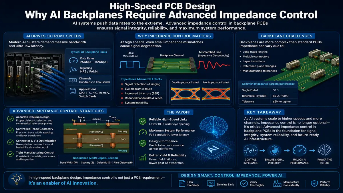
High-Speed PCB Design: Why AI Backplanes Require Advanced Impedance Control
Technical Insights into High-Speed PCB Signal Integrity for Next-Generation AI Server Infrastructure
Table of Contents
- 1. Introduction: The Critical Role of AI Server Backplanes
- 2. Demystifying Advanced Impedance Control (Transmission Line Theory)
- 3. Uncompromising Technical Requirements of AI Backplane PCBs
- 4. Why AI Backplanes Demand Advanced Impedance Control
- 5. Core Design Strategies for High-Precision Impedance Control
- 6. Signal Integrity Simulation and TDR/VNA Testing Methodologies
- 7. Manufacturing and DFM Challenges in Ultra-Layer Backplane Fabrication
- 8. Future Trends: From 448G Interconnects to Glass Substrates
- 9. Strategic Optimization Summary for AI Hardware Engineers
- 10. High-Speed PCB Procurement FAQ
1. Introduction: The Critical Role of AI Server Backplanes
The explosive global expansion of generative AI, large language models (LLMs), and hyper-scale neural network training workloads has fundamentally disrupted hardware architecture. Traditional data center infrastructures are no longer capable of keeping pace with the massive parallel processing data rates required by state-of-the-art GPU cluster fabrics.
Within an AI server architecture, the backplane PCB acts as the central central-nervous-system highway. It handles high-density, intra-system data exchanges between GPU accelerators, switch matrices, CPU host nodes, and high-speed storage sub-systems. Because computing nodes parse data into smaller parallel threads that require tight coherency, any system-level latency or transmission error degrades overall cluster efficiency.
As a result, managing high-speed PCB design parameters has shifted from a standard engineering check-box to a critical operational priority. At the center of this paradigm shift is impedance control, the foundational discipline required to guarantee hardware reliability under relentless high-frequency data loads.
2. Demystifying Advanced Impedance Control (Transmission Line Theory)
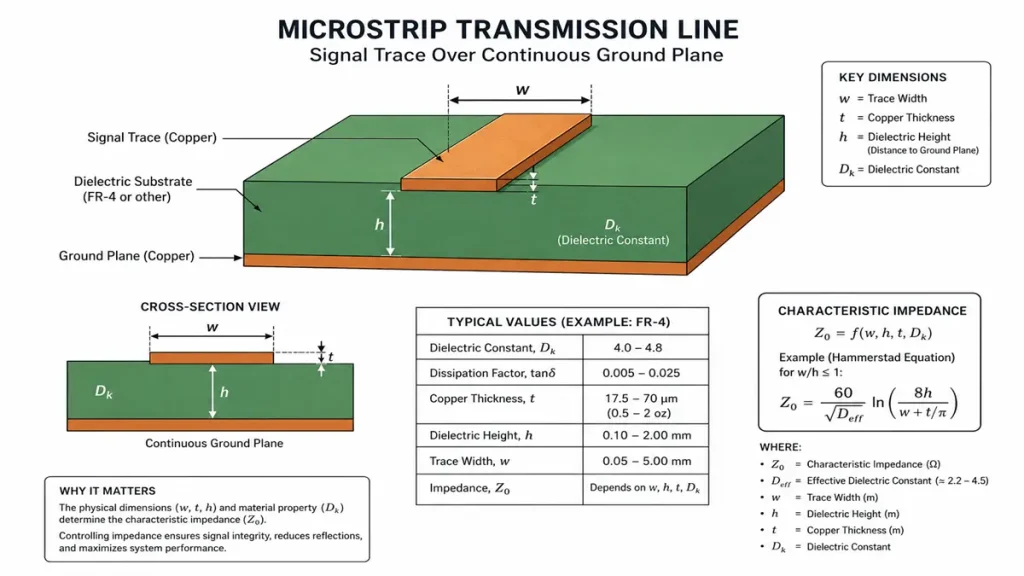
Cross-sectional microstrip transmission line model utilized by PCBKR for controlled impedance simulation. Variables W1/W2 (trace width), T1 (copper thickness), H1 (dielectric height), and Er1 (Dk / dielectric constant) are precisely calculated to achieve a target 50-ohm or 100-ohm differential impedance
In low-frequency electronic circuit design, PCB traces function as simple connecting wires. However, when the rise time of an operating digital signal is shorter than the time it takes to travel across the trace, the connection must be treated as a transmission line.
                       [Signal Trace: Width (w), Thickness (t)]
                 ─────────────────────────────────────────────
                   ↑  Dielectric Constant (Dk) / Prepreg (h)
                 ─────────────────────────────────────────────
                       [Reference Plane: Continuous GND]
Advanced impedance control is the precise balancing of a trace’s physical geometries and material properties. This ensures that the characteristic impedance (Z₀) remains entirely uniform along the entire length of the signal transmission path. Mathematically, characteristic impedance is governed by the structural relation of the line’s inherent inductance (L), capacitance (C), resistance (R), and conductance (G):
Z₀ = √( (R + jωL) / (G + jωC) )
For multi-GHz high-frequency operations, where resistance and conductance become secondary to reactive components (R ≪ ωL and G ≪ ωC), the equation simplifies to its high-frequency approximation:
Z₀ ≈ √(L / C)
Standard Impedance Profiles in Modern AI Subsystems
Modern high-speed PCB design and fabrication balances distinct impedance targets based on target interface standards:
- 50Ω Single-Ended Lines: Utilized for specialized RF instrumentation, clock distributions, and single-ended legacy test nodes.
- 85Ω Differential Pairs: The standard architecture adopted by Intel, AMD, and PCIe Gen 5 / PCIe Gen 6 architectures to lower driver power consumption and optimize routing space.
- 100Ω Differential Pairs: The baseline infrastructure for traditional Ethernet protocols, InfiniBand networks, and high-speed SerDes communication lines.
3. Uncompromising Technical Requirements of AI Backplane PCBs
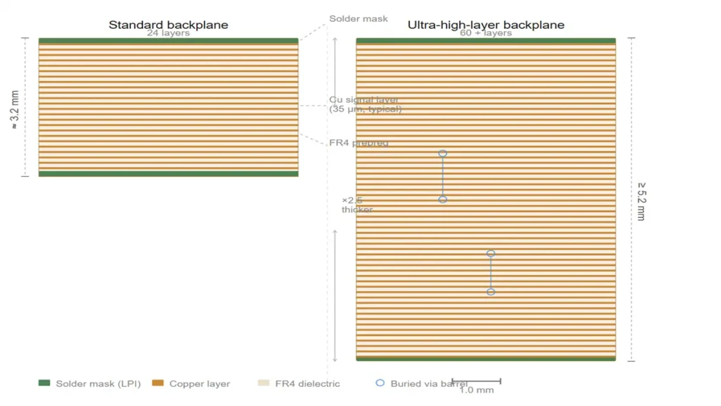
Cross-Section Comparison: Standard 24-Layer vs. Ultra-High-Layer (60+ Layers) Backplane PCB Architecture.
Designing an AI server backplane substrate presents severe layout and material challenges that exceed standard enterprise server layouts.
- Ultra-High-Speed Signaling (112G and 224G PAM4): Moving from NRZ (Non-Return-to-Zero) to PAM4 signaling quadruples data throughput by packing 2 bits of data into 4 discrete voltage levels per symbol. However, this reduces the signal-to-noise ratio (SNR) by -9.54 dB, making the interconnect channel exceptionally sensitive to minor signal impairments.
- High-Density Interconnects (HDI) & Heavy Layer Counts: AI backplanes routinely scale from 24 to over 60 layers, often exceeding a total board thickness of 5.0 mm. Managing trace configurations within tightly packed ball grid array (BGA) breakouts requires advanced high-density interconnect (HDI) strategies.
- Extended Physical Routing Reach: Unlike compact add-in accelerator modules, backplanes must route clean data lines over long physical spans—often stretching from 30 to over 70 cm across thick boards to connect midplanes, backplanes, and orthogonal mezzanine cards.
4. Why AI Backplanes Demand Advanced Impedance Control
When multi-gigabit SerDes streams encounter even small physical shifts along a transmission line, the high frequency turns minor geometry changes into major barriers to signal transmission.
The Impact of Impedance Discontinuities
Any variance from the target characteristic impedance (Z₀) creates an impedance mismatch. The severity of the resulting signal reflection is calculated using the voltage reflection coefficient (Γ):
Γ = (Z_L – Z₀) / (Z_L + Z₀)
Where Z_L represents the load impedance at the discontinuity point. If a 100Ω transmission pair hits an uncompensated via or a poorly fabricated layer transition that drops to 80Ω, a significant portion of the high-frequency wave reflects back to the source. This creates standing waves and disruptive signal integrity failures in AI server architectures.
Signal Integrity Deficiencies: Reflection, Crosstalk, and ISI
- Reflections and Resonance: Reflected waves combine destructively with the forward-traveling bit stream, causing severe attenuation and ripple artifacts in the channel response.
- Crosstalk (FEXT / NEXT): In tightly packed differential line channels, any impedance variance increases electromagnetic energy leakage into adjacent lanes, causing high forward and backward crosstalk.
- Intersymbol Interference (ISI): Energy delays from multiple reflection loops smear data pulses into adjacent bit intervals, closing the vertical and horizontal margins of the PAM4 signal eye diagram.
Minimizing Bit Error Rates (BER)
AI computing clusters rely heavily on parallel computing efficiency. Because there is little system overhead available to re-send dropped packets, hardware systems demand an incredibly low baseline Bit Error Rate (BER)—typically 10⁻¹² to 10⁻¹⁵. Advanced impedance control directly protects this margin by stabilizing signal amplitude and phase alignment.
5. Core Design Strategies for High-Precision Impedance Control
To achieve ultra-precise differential impedance control within a strict ±5% tolerance, engineers must carefully optimize every layer of the system stackup.
1. Advanced Low-Loss PCB Materials Selection
Standard FR4 laminates degrade high-frequency signals due to high dielectric loss. Designers must specify very-low-loss or ultra-low-loss resin materials (with a Dissipation Factor D_f ≤ 0.002 and a Dielectric Constant D_k ≤ 3.5), choosing premium backplane PCB materials like Megtron 6, Megtron 7, or Tachyon 100G.
Furthermore, at 56 GHz Nyquist frequencies (for 112G SerDes) and 112 GHz (for 224G SerDes), the skin effect forces current to flow entirely along the outer edge of the trace. Standard copper foil profiles introduce high inductive loss due to surface roughness. Designers should specify HVLP (Hyper Very Low Profile) or VLP2 copper foils to minimize this high-frequency resistance.
2. Precise Trace Geometry and Stackup Optimization
- Trace Configurations: Stripline configurations sandwiched between continuous ground reference planes are required for critical high-speed routing to ensure maximum EMI shielding and stable reference profiles.
- Glass Weave Mitigation: To prevent phase skew caused by the uneven weave of fiber-glass fabrics (the cavity effect between glass bundles and resin pockets), designers use spread-glass or angled routing strategies (7° to 12° relative to the panel weave direction).
3. Via Engineering and Advanced Backdrill Technology
Vertical transitions through vias are a common source of impedance disruptions. An unused via barrel extension acts as an open-ended stub, creating a capacitive resonance trap.
       UNCOMPENSATED VIA                    BACKDRILLED VIA
     ┌───┐            ┌───┐               ┌───┐            ┌───┐
 ────┤   ├────────────┤   ├────       ────┤   ├────────────┤   ├────  [Signal]
     │   │            │   │               │   │            │   │
     │ █ │ <-- Stub   │ █ │               │   │            │   │
     │ █ │    Resonance│ █ │              │   │            │   │
     └───┘            └───┘               └───┘            └───┘  [Stub Removed]
To counter this, engineers specify precision backdrilling depth control to remove unused copper stubs, keeping the remaining stub length under 0.2 mm (or within 1/20 of the resonant signal wavelength).
6. Signal Integrity Simulation and TDR/VNA Testing Methodologies
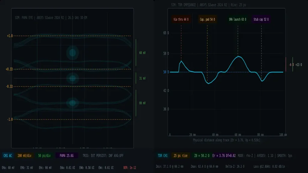
TDR Impedance Profile over a 100 mm physical trace simulation (ANSYS SIwave 2024 R2), mapping impedance fluctuations ($\Omega$) caused by a via, capacitor pad, SMA launch, and stub at a 25 ps rise time.
Validating a complex high-speed interconnect layout requires a mix of pre-layout emulation and strict post-production validation.
Pre-Layout and Post-Layout EDA Simulation
Design teams model the entire interconnect system using advanced 3D Electromagnetic Field Solvers, such as Ansys HFSS, Synopsys PrimeSim, or Cadence Sigrity. These tools extract S-parameter matrices, model signal attenuation profiles, and simulate synthetic PAM4 eye diagrams to catch layout bottlenecks before manufacturing begins.
Post-Fabrication Physical Verification
| Testing Technology | Core Instrument Used | Primary Measurement Metric |
|---|---|---|
| TDR (Time Domain Reflectometry) | High-Sampling Digital Sampling Oscilloscope | Locates structural impedance variations (Ω) over physical distance (mm). |
| VNA (Vector Network Analysis) | Multi-port Vector Network Analyzer | Measures insertion loss (S₂₁), return loss (S₁₁), and crosstalk profiles across frequency spectrums up to 110 GHz. |
7. Manufacturing and DFM Challenges in Ultra-Layer Backplane Fabrication
Even a perfect layout can fail if the production process isn’t tightly controlled. Fabricating thick, high-layer-count boards requires deep alignment with your manufacturer’s Design for Manufacturability (DFM) guidelines.
- Etching and Dielectric Tolerances: Variations in etching can alter trace cross-sections from an ideal rectangle to a trapezoid, lowering the final impedance. Advanced fabricators use laser direct imaging (LDI) and automated optical shaping to keep trace width variations within ±10μm.
- Multilayer Lamination Alignment: Pressing over 30 layers of varying prepregs and cores can cause core shifting or internal warpage. Advanced registration systems and dynamic press profiling are critical to keeping layer-to-layer registration alignment within ±2 mils.
- Controlled Impedance Coupon Verification: Every production panel must include dedicated testing coupons at its outer edges. These coupons undergo 100% TDR validation to confirm the structural quality of the main production board.
8. Future Trends: From 448G Interconnects to Glass Substrates
As data demands continue to scale, hardware architectures are evolving rapidly to support next-generation workloads.
- The Leap to 224G and 448G Architectures: Next-generation AI networks are shifting from 112G to 224G SerDes platforms, with 448G research already underway. At these frequencies, traditional PCB traces become highly restrictive over standard distances, driving the adoption of “Flyover” twinaxial cable systems that route signals directly above the board surface.
- CPO (Co-Packaged Optics) Integration: Co-Packaged Optics move optical transceivers directly onto the compute substrate next to the GPU/ASIC cluster. This shortens the electrical transmission length to a few millimeters, radically reducing insertion loss and simplifying board routing.
- Alternative Core Materials: To overcome the high-frequency limits of organic resins and glass fibers, the industry is exploring ultra-stable materials like glass substrates and advanced ceramics. These offer exceptional dimensional stability, low dielectric losses, and ultra-smooth surface tracking for high-frequency signals.
9. Strategic Optimization Summary for AI Hardware Engineers
Achieving reliable signal transmission in next-generation AI platforms requires a systematic approach to system design:
  [Material Selection]  ──>  [Geometry Engineering] ──>  [DFM Collaboration]
  - Ultra-low loss resin      - Stripline routing         - Extreme backdrill limits
  - HVLP copper foils         - Broad spread-glass weave  - Strict ±5% TDR validation
By combining advanced 3D EM simulation with strict manufacturing controls, hardware teams can prevent signal degradation and deliver the high-performance throughput that modern AI data centers demand.
High-Speed PCB Procurement FAQ
What standard impedance tolerance should I specify for high-speed AI backplane fabrication?
While the industry standard for standard boards is ±10%, high-speed AI server backplanes handling 112G/224G PAM4 signaling require a strict ±5% differential impedance tolerance to minimize signal reflections and maintain target bit error rates (BER).
Which ultra-low-loss PCB laminates are recommended for 112G and 224G SerDes applications?
For high-frequency AI infrastructures, procurement teams should look for ultra-low-loss laminates with a Dissipation Factor (Df) ≤ 0.002. Leading industry choices include Panasonic Megtron 6 / Megtron 7, Isola Tachyon 100G, and Doosan DS-7409DV.
Why is backdrilling essential for heavy layer-count AI server backplanes, and what are the procurement limits?
In thick boards (often over 5.0 mm with 24 to 60+ layers), via stubs create signal-destroying capacitive resonances. Precision backdrilling removes these unused copper stubs. When sourcing, ensure your manufacturer can consistently maintain a remaining stub length of under 0.2 mm.
How does copper foil surface roughness impact the price and performance of high-layer PCB panels?
At multi-gigahertz frequencies, the skin effect forces current to travel along the outer edge of the trace. Standard rough copper foil increases attenuation. Specifying HVLP (Hyper Very Low Profile) or VLP2 copper foils minimizes this loss and is vital for signal integrity, though it carries a cost premium over standard RTF (Reverse Treated Foil).
What physical verification reports should a buyer request from a high-speed PCB manufacturer?
To verify structural quality, buyers should require a 100% TDR (Time Domain Reflectometry) test report for impedance validation, microsection analysis reports to verify lamination alignment/layer registration, and VNA (Vector Network Analyzer) insertion loss test data on dedicated panel coupons.
Using top-tier AI server PCB equipment to manufacture traditional PCBs delivers a strategic advantage: interlayer alignment tolerance shrinks from ±75μm to within ±25μm, and differential impedance control tightens to ±5%. Paired with 100% 3D X-Ray inspection, it grants conventional boards chip-level precision, superb signal stability, and near-100% yield.
Still, need help? Contact Us: sales@pcbkr.com
Need a PCB or PCBA quote? Quote now
About Author
David Chen https://www.linkedin.com/in/pcbcoming
David Chen boasts an extensive professional background in PCBA manufacturing, PCBA testing, and PCBA optimization, with specialized expertise in high-precision PCBA fault analysis and rigorous PCBA reliability testing. Skilled in complex circuit design and cutting-edge advanced PCB manufacturing processes, he delivers solutions that elevate product durability and performance across industrial applications. His technical articles focusing on PCBA manufacturing workflows and testing methodologies are widely cited by industry peers, research institutions, and technical platforms, solidifying his reputation as a recognized technical authority in the global circuit board manufacturing sector.