What Is a Multilayer PCB? A 2026 Guide to Core, Prepreg & Lamination
In the fast-evolving world of electronics, multilayer PCBs (Printed Circuit Boards) have become the backbone of advanced devices—from smartphones to aerospace systems. This guide breaks down the fundamentals of multilayer PCBs, their structure, and the lamination process that brings them to life. Whether you’re a hobbyist, engineer, or industry professional, this article will help you grasp the basics of multilayer PCB design, core, prepreg, and stackup.
What Is a Multilayer PCB?
A multilayer PCB is a type of printed circuit board that consists of three or more conductive copper layers bonded together with insulating materials. Unlike single-layer or double-layer PCBs, which have conductive layers on one or both sides of a single substrate, multilayer PCBs stack multiple layers of circuitry, interconnected through vias (small holes plated with conductive material).
Why Multilayer PCBs?
As electronic devices become more compact and complex, the demand for higher circuit density and better signal integrity grows. Multilayer PCBs address these needs by:
- Saving space: Allowing more circuitry to fit into a smaller footprint.
- Improving performance: Reducing electromagnetic interference (EMI) and crosstalk between components.
- Enhancing reliability: Providing better heat dissipation and mechanical stability.
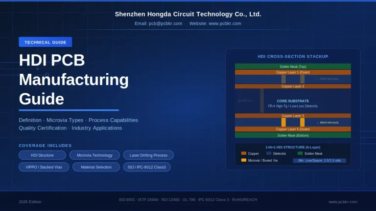
The Building Blocks: Core and Prepreg in Multilayer PCBs
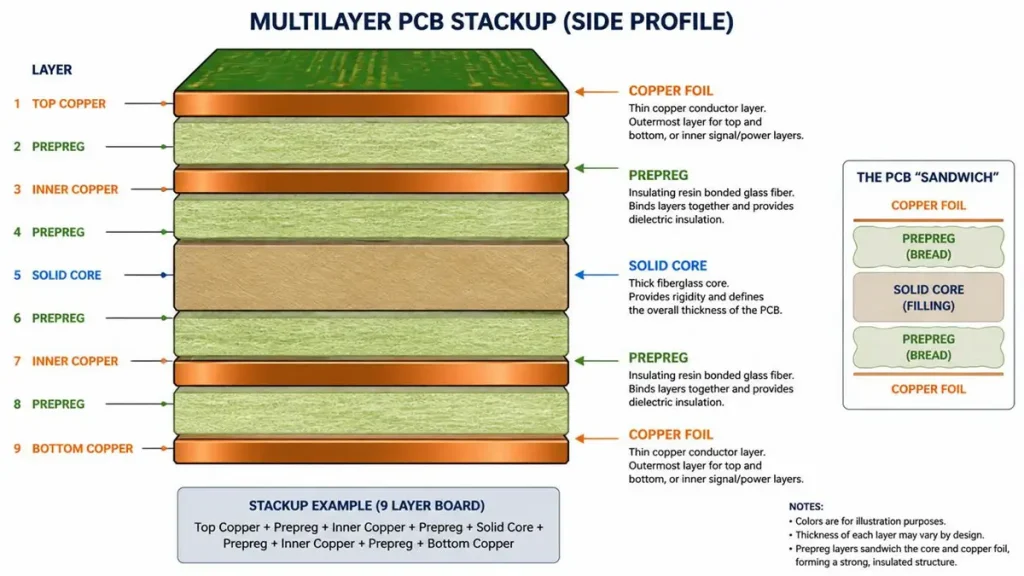
A detailed look at a multilayer PCB stackup profile, highlighting how prepreg and solid core layers function like a “sandwich” to support copper circuitry.
To understand how multilayer PCBs are constructed, it’s essential to familiarize yourself with two critical components: Core and Prepreg.
What Is a Core in a PCB?
The core is the rigid, central layer of a multilayer PCB. It is typically made of fiberglass-reinforced epoxy resin (FR-4) and is pre-coated with copper foil on both sides. The core provides the structural foundation for the PCB, ensuring mechanical stability and acting as the primary layer for circuit tracing.
Key Characteristics of Core:
- Double-sided copper cladding: Both sides of the core are covered with copper, allowing for circuitry on both surfaces.
- Rigid and durable: The core is fully cured, meaning it is solid and does not change shape under normal conditions.
- Thickness options: Cores come in various thicknesses, typically ranging from 0.2mm to 3.2mm, depending on the application.
What Is Prepreg in a PCB?
Prepreg, short for pre-impregnated fiberglass, is a semi-cured epoxy resin material used to bond the core layers together. Unlike the core, prepreg is not fully hardened—it is in a B-stage state, meaning it is partially cured and can still flow when subjected to heat and pressure during the lamination process.
Key Characteristics of Prepreg:
- Adhesive properties: Prepreg acts as a bonding agent, holding the core layers together.
- Insulating material: It provides electrical insulation between the conductive layers.
- Fills gaps: During lamination, prepreg flows to fill any irregularities, ensuring a smooth and uniform bond.
How Are Multilayer PCBs Made? The Lamination Process
The manufacturing of multilayer PCBs involves a layer-by-layer lamination process, where cores and prepregs are stacked and bonded under heat and pressure. Here’s a simplified breakdown of the multilayer PCB fabrication process as practiced by industry leaders in 2026:
Step 1: Inner Layer Preparation
- Copper Cladding: Start with a core material that has copper foil on both sides.
- Circuit Etching: Use a photolithography process to etch the desired circuit pattern onto the copper layers of the core.
- Inspection: Inspect the inner layers for defects to ensure quality.
Step 2: Layer Stackup
- Stacking: Alternate layers of core and prepreg in the desired configuration.
- Alignment: Ensure precise alignment of all layers to prevent misregistration.
Step 3: Lamination
- Heat and Pressure: Place the stacked layers in a lamination press and apply heat (typically 170–190°C) and pressure (200–400 psi).
- Curing: The prepreg melts and flows, bonding the layers together. The epoxy resin fully cures, turning the stack into a single, solid PCB.
- Cooling: Gradually cool the laminated board to room temperature.
Step 4: Drilling and Plating
- Drilling: Drill holes for vias to create electrical connections between layers.
- Desmearing: Remove any resin residue from the drilled holes.
- Copper Plating: Plate the walls of the holes with copper to ensure conductivity between layers.
Step 5: Outer Layer Processing
- Copper Deposition: Add a thin layer of copper to the outer surfaces of the board.
- Circuit Etching: Etch the outer layer circuits using the same photolithography process.
- Solder Mask Application: Apply a solder mask to protect the copper traces and prevent solder bridges.
Step 6: Finishing Touches
- Surface Finish: Apply a surface finish (e.g., HASL, ENIG, or OSP) to protect the copper and improve solderability.
- Testing: Perform electrical testing to ensure all circuits are functioning correctly.
- Final Inspection: Inspect the PCB for any defects or imperfections.
Understanding Multilayer PCB Stackup: The “Sandwich” Analogy
To visualize the structure of a multilayer PCB, think of it as a multi-level sandwich:
- Bread Slices (Core): The rigid, structural layers that hold the “filling” (circuitry) in place.
- Condiments (Prepreg): The sticky, insulating layers that bond the bread slices together and keep the filling from mixing.
- Fillings (Copper Layers): The conductive layers where the actual circuits are etched.
Why Use Multilayer PCBs? Key Applications
Multilayer PCBs are the go-to choice for applications that demand high performance, compactness, and reliability. Here are some of the most common use cases:
1. Consumer Electronics
- Smartphones and Tablets: Multilayer PCBs enable the miniaturization of components while maintaining high performance.
- Wearable Devices: Compact and lightweight, multilayer PCBs are ideal for smartwatches and fitness trackers.
2. Industrial Equipment
- Control Systems: Used in automation and robotics for precise and reliable circuit control.
- Power Supplies: Multilayer PCBs help manage high voltage and current efficiently.
3. Medical Devices
- Diagnostic Equipment: Multilayer PCBs are used in MRI machines, ultrasound devices, and patient monitors for their reliability and precision.
- Implantable Devices: Compact and durable, multilayer PCBs are essential for pacemakers and hearing aids.
4. Automotive Industry
- Engine Control Units (ECUs): Multilayer PCBs are used in vehicle electronics for engine management, safety systems, and infotainment.
- Electric Vehicles (EVs): High-power multilayer PCBs are critical for battery management systems (BMS) and charging infrastructure.
5. Aerospace and Defense
- Avionics: Multilayer PCBs are used in flight control systems, radar, and communication equipment for their ability to withstand extreme conditions.
- Satellites: The high reliability and compactness of multilayer PCBs make them ideal for space applications.
Multilayer PCB vs. Single-Layer and Double-Layer PCBs
| Feature | Single-Layer PCB | Double-Layer PCB | Multilayer PCB |
| Number of Layers | 1 | 2 | 3 or more |
| Complexity | Low | Moderate | High |
| Space Efficiency | Low | Moderate | High |
| Cost | Low | Moderate | High |
| Performance | Basic | Improved | Advanced |
| Applications | Simple circuits | Moderate circuits | Complex circuits |
The Future of Multilayer PCBs: Trends in 2026
The PCB industry is constantly evolving, and 2026 brings exciting advancements in multilayer PCB technology. Here’s what’s shaping the future:
1. HDI (High-Density Interconnect) PCBs
- Finer Pitch: Components are getting smaller, requiring higher density interconnects.
- Advanced Via Technologies: Laser-drilled microvias enable more complex designs in smaller spaces.
2. Flexible and Rigid-Flex PCBs
- Wearable Tech: The demand for flexible and foldable devices is driving innovation in flexible PCBs.
- 3D Printing: Additive manufacturing is being explored for creating custom PCB designs.
3. Sustainable Materials
- Eco-Friendly Resins: Manufacturers are adopting bio-based and recyclable materials to reduce environmental impact.
- Lead-Free Processes: Compliance with RoHS (Restriction of Hazardous Substances) is becoming standard.
4. AI and Automation in Manufacturing
- Smart Factories: AI-driven quality control and automated assembly lines are improving efficiency and reducing defects.
- Predictive Maintenance: Machine learning is used to predict equipment failures and optimize production schedules.
5. 5G and IoT Applications
- High-Frequency PCBs: The rollout of 5G networks requires PCBs capable of handling high-frequency signals with minimal loss.
- IoT Devices: The proliferation of IoT devices demands compact, reliable, and cost-effective multilayer PCBs.
How to Choose the Right Multilayer PCB Manufacturer
Selecting the right manufacturer is crucial for ensuring the quality, reliability, and performance of your multilayer PCBs. Here’s what to look for in a trusted PCB supplier like Shenzhen Hongda Circuit Technology Co., Ltd.:
1. Experience and Expertise
- Industry Reputation: Look for manufacturers with a proven track record in producing high-quality multilayer PCBs.
- Technical Support: Ensure the manufacturer offers expert guidance on design, material selection, and manufacturing.
2. Manufacturing Capabilities
- Layer Count: Check if the manufacturer can handle the number of layers your design requires.
- Material Options: Ensure they offer a wide range of materials to suit your application.
- Advanced Technologies: Look for capabilities in HDI, flexible PCBs, and rigid-flex PCBs.
3. Quality Control
- Certifications: Ensure the manufacturer adheres to industry standards such as ISO 9001, UL, and RoHS.
- Testing Methods: Verify that they use advanced testing methods like AOI, flying probe testing, and impedance testing.
4. Turnaround Time and Cost
- Lead Time: Consider the manufacturer’s production lead time to meet your project deadlines.
- Pricing: Compare pricing to ensure it fits your budget without compromising on quality.
5. Customer Support
- Responsive Service: Choose a manufacturer that offers excellent customer support and clear communication.
- After-Sales Service: Ensure they provide reliable after-sales support for any issues that may arise.
Conclusion: Mastering the Basics of Multilayer PCBs
Multilayer PCBs are the backbone of modern electronics, enabling the creation of compact, high-performance, and reliable devices. Understanding the role of core and prepreg, the lamination process, and the design best practices is essential for anyone working with or designing multilayer PCBs.
At Shenzhen Hongda Circuit Technology Co., Ltd., we specialize in high-quality multilayer PCB manufacturing, leveraging the latest 2026 technologies to deliver innovative, reliable, and cost-effective solutions. Whether you’re a hobbyist, engineer, or industry professional, we’re here to support your PCB needs with expertise, precision, and excellence.
FAQ
What core materials and options do you offer for multilayer PCB manufacturing?
We utilize high-quality fiberglass-reinforced epoxy resin (FR-4) as our standard rigid core material, which provides excellent mechanical stability and pre-coated copper cladding. Depending on your application’s requirements, our core thicknesses typically range from 0.2mm to 3.2mm. We also offer advanced material options to suit high-frequency (5G), IoT, and eco-friendly applications.
Can your factory handle advanced layer stackups and lamination for complex designs?
Yes. We specialize in precise layer-by-layer lamination processes, alternating cores and semi-cured prepreg bonding agents under strict heat (170–190°C) and pressure (200–400 psi) controls. This ensures flawless resin flow, zero misregistration, and an optimal “sandwich” structure for high-density, multi-layer circuit designs.
Do you support High-Density Interconnect (HDI) and microvia technologies?
Absolutely. To meet the 2026 electronics trend of shrinking components and finer pitches, we offer advanced HDI PCB manufacturing. This includes precision laser-drilled microvias, enabling high-performance routing in much smaller footprints for consumer electronics and medical devices.
What quality assurance testing methods do you perform on multilayer PCBs?
Quality is our top priority. Our multi-step inspection includes Inner Layer Inspection before lamination, and comprehensive end-of-line testing such as AOI (Automated Optical Inspection), flying probe testing, and impedance testing to guarantee signal integrity and eliminate defects.
What international certifications does your PCB manufacturing plant hold?
As a reliable industry leader, our manufacturing processes strictly adhere to global standards. We are fully certified in ISO 9001 for quality management, UL for safety, and comply entirely with RoHS guidelines (lead-free processes and eco-friendly resins).
About Author
David Chen https://www.linkedin.com/in/pcbcoming
David Chen boasts an extensive professional background in PCBA manufacturing, PCBA testing, and PCBA optimization, with specialized expertise in high-precision PCBA fault analysis and rigorous PCBA reliability testing. The author has worked with high-layer-count server PCB fabrication, ultra-low-loss backplane stackups, and thermo-mechanical reliability optimization for AI infrastructure projects involving 112G and 224G PAM4 architectures. Skilled in complex circuit design and cutting-edge advanced PCB manufacturing processes, he delivers solutions that elevate product durability and performance across industrial applications. His technical articles focusing on PCBA manufacturing workflows and testing methodologies are widely cited by industry peers, research institutions, and technical platforms, solidifying his reputation as a recognized technical authority in the global circuit board manufacturing sector.