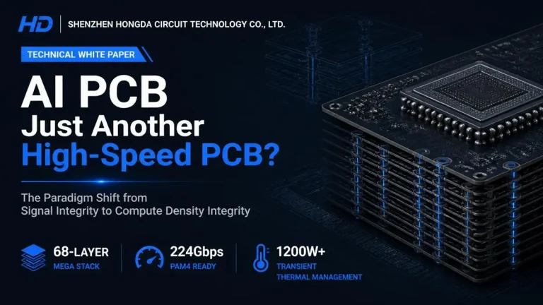
Why AI Servers Demand Higher PCB Layer Counts
When evaluating the infrastructure powering next-generation data centers, one critical engineering requirement stands out: AI servers demand a significantly higher PCB layer count compared to traditional enterprise systems. As artificial intelligence workloads scale exponentially, standard multi-layer boards can no longer sustain the extreme signal speeds, structural densities, and power topologies required by modern accelerator complexes.
To help infrastructure architects, hardware engineers, and procurement teams navigate these technological shifts, this guide analyzes why upgrading to an ultra-high layer count PCB architecture is now mandatory for AI hardware deployment.
Executive Summary: The AI PCB Evolution at a Glance
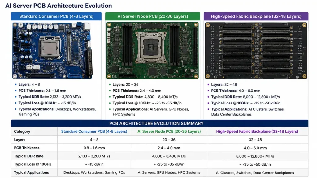
PCB Architecture Evolution from Consumer to AI Fabric Backplanes
For engineering and procurement professionals evaluating hardware suppliers, this architectural breakdown highlights the evolution across computing generations:
| Generation | Average Layer Count | Dominant Material Systems | Key Interconnects | Primary Design Bottleneck |
|---|---|---|---|---|
| Standard Enterprise Server | 4 to 8 layers | Standard FR-4 | PCIe 3.0 / 4.0 | Manufacturing Cost |
| High-Performance Computing (HPC) | 12 to 16 layers | Mid-Loss / High-Tg Standard | PCIe 5.0 | Signal Attenuation |
| Next-Gen AI Train/Inference (e.g., Blackwell/Rubin Clusters) | 28 to 36+ layers (Backplanes up to 48+) | Panasonic Megtron 7 / Megtron 8, Rogers High-Frequency Alloys | 224G PAM4, NVLink 5/6, PCIe 6.0/7.0 | 56GHz Signal Integrity, Warpage & IR Drop |
1. What Defines an Ultra-High Layer Count PCB in AI Architecture?
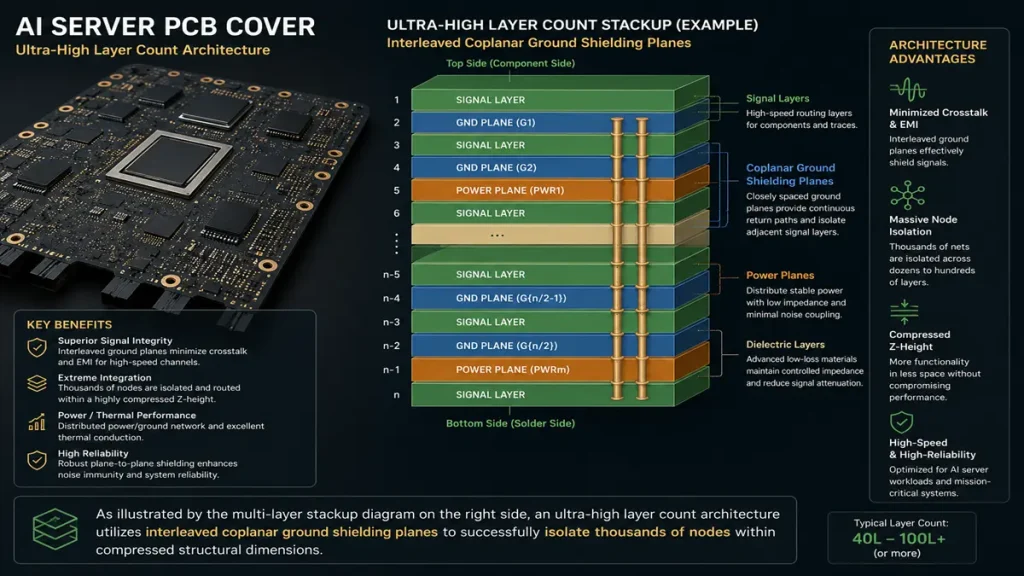
Cross-Sectional View of an Ultra-High Layer Count PCB Stackup
In high-performance AI computing, an ultra-high layer count PCB is defined as a highly integrated substrate incorporates 28 to 48+ structural layers. These are interleaved with advanced, ultra-low-loss dielectric materials designed to handle dense routing topologies.
Traditional server motherboards rely on simpler routing pathways. In contrast, AI hardware topologies—such as Universal Baseboards (UBB) and OAM accelerator modules—utilize complex layer stackups to accommodate tens of thousands of individual node connections. By isolating high-speed differential signal traces from massive power distribution networks (PDNs) using dedicated coplanar ground shielding planes, these boards allow hardware engineers to compress immense computing density into standard rack dimensions without inducing destructive cross-talk.
2. Key Technical Drivers: The Move to 224G PAM4 and Parallel Scaling
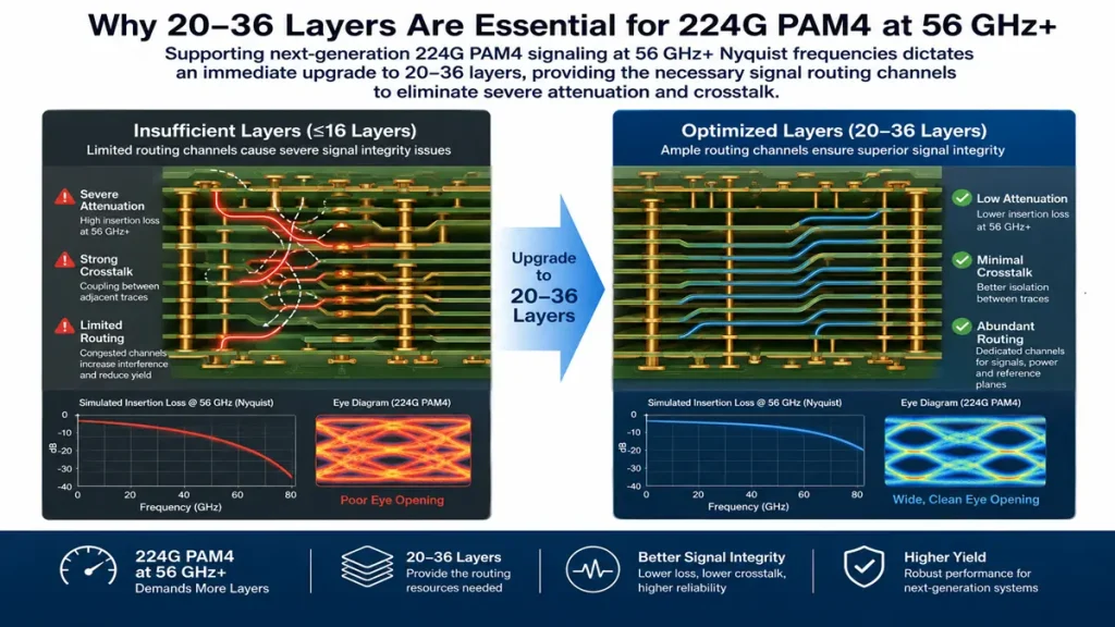
Impact of Layer Count Optimization on 224G PAM4 Signal Integrity
224G PAM4 Signaling and GPU Interconnects
Modern AI clusters rely on massive parallel computing architectures where multiple clusters of GPUs or TPUs must communicate simultaneously with near-zero latency. With the transition from 112G to 224G PAM4 signaling protocols, the Nyquist frequency jumps to 56 GHz and above.
At these extreme frequencies, traditional PCB routing causes catastrophic signal attenuation. To prevent data degradation, separate ultra-high-speed signal paths must be meticulously isolated on individual internal layers. This isolation allows clean routing between processors without phase distortion or insertion loss.
BGA Density and Modified Semi-Additive Processes (mSAP)
The physical footprint of an AI accelerator board is densely crowded, hosting multiple processor sockets, multi-channel high-bandwidth memory (HBM3e/HBM4), and high-speed switch chips. This density creates an enormous concentration of fine-pitch Ball Grid Array (BGA) components.
To clear thousands of BGA pins, designers use advanced High-Density Interconnect (HDI) structures combined with Any-Layer Any-Via configurations. When trace/space requirements drop below 30/30 μm, traditional subtractive etching fails. Fabricators must implement modified Semi-Additive Processes (mSAP) across 30+ layers to ensure precise trace geometry and accurate escape routing.
3. Engineering Performance and Stackup Advantages
Precision Impedance Management at 56 GHz+
Signal Integrity Focus: Operating at frequencies above 56 GHz demands rigid impedance control, often within a strict ±5% tolerance. By using ultra-thin dielectric materials and hyper-low-profile (HVLP) copper foils across a 32-layer stackup, engineers minimize skin effect losses and signal reflections, preserving the eye diagram integrity of high-speed paths.
Faraday Cage Shielding and EMI Mitigation
With billions of data transitions occurring every second, AI servers generate massive electromagnetic fields. An advanced multi-layer stackup allows designers to sandwich critical signal layers between solid copper ground planes. This stripline configuration creates an internal Faraday cage effect, delivering enhanced electromagnetic interference (EMI) shielding that protects delicate differential data lines from system-generated noise.
Power Delivery Network (PDN) Stability against IR Drop
Next-generation AI accelerators pull over 1,000 Watts per socket during peak Large Language Model (LLM) training cycles. Delivering thousands of amperes of current at sub-1V levels without severe voltage drops (IR Drop) requires a robust Power Distribution Network.
Ultra-high layer count boards solve this by dedicating multiple heavy copper internal layers (up to 2oz or 3oz copper) exclusively to power and ground planes. This setup minimizes DC resistance and ensures clean, stable transient power delivery under sudden, intense computational spikes.
4. Advanced Manufacturing Realities and Supply Chain Challenges
While the performance benefits are clear, scaling up the layer count introduces complex manufacturing variables that procurement teams must carefully manage:
- Registration and Layer Realities: Laminating 32 or more layers of ultra-thin material requires extreme precision. Controlling registration errors and misalignments across multiple pressing cycles directly impacts yield rates and fabrication costs.
- Material System Material Demands: Traditional FR-4 systems are entirely obsolete in this space. Fabricators must utilize specialized ultra-low-loss laminates like Panasonic Megtron 7/8 or Rogers high-frequency systems to handle continuous high-temperature workloads without risking delamination.
- Thermal Coefficent & Warpage Management: Thick, dense multi-layer boards act as thermal insulators. Managing the heat dissipating from internal power planes requires deep expertise in thermal management, often necessitating integrated liquid cooling blocks, specialized thermal vias, or thick embedded copper coins to combat PCB warpage during assembly reflow.
Technical FAQ (Hardware Procurement Guide)
What is the upper limit of layers for modern AI hardware platforms?
Currently, mainstream AI accelerator baseboards and high-density GPU modules utilize 28 to 36 layers as a standard configuration. For ultra-dense AI supercomputing backplanes and high-speed fabric switch boards, advanced fabricators routinely scale custom manufacturing capabilities up to 48 or even 64 layers to meet complex routing demands.
Why are traditional through-hole vias inadequate for 224G PAM4 routing?
Traditional through-hole vias create large vertical stubs that cause severe capacitive reflections and signal degradation at high frequencies. At 224G PAM4 (56 GHz+), these stubs must be completely eliminated. Engineers use blind, buried, and precisely backdrilled vias to remove unused via stubs, preserving signal paths across the internal layers.
How do hybrid stackups balance heavy power delivery with high-frequency signaling?
AI server boards use complex hybrid stackups. Dedicated power layers use heavy copper to maximize current carrying capacity and reduce DC resistance. Conversely, high-speed signal layers use ultra-thin copper foils and specialized low-Dk/Low-Df dielectrics to support high-density, fine-pitch trace routing without signal loss.
6. Future Trends: Advanced Packaging and AI-Driven Layouts
As AI models expand to trillions of parameters, hardware demands will intensify. The industry is shifting toward closer integration of advanced packaging technologies, such as Chip-on-Wafer-on-Substrate (CoWoS), directly interfacing with system-level high-density multilayer PCB architectures.
Furthermore, EDA software is increasingly utilizing AI-driven routing optimization tools to calculate optimal layer configurations and trace paths, solving complex signal integrity anomalies that would take human engineers weeks to simulate. Ultimately, the trajectory is clear: as AI computing demands scale, the dependency on complex, ultra-high-layer count printed circuit boards will remain a cornerstone of next-generation infrastructure development.
Overcoming the Challenges of 224G PAM4 and Ultra-High Layer Count PCBs?
Navigating 32+ layer registration, advanced mSAP processing, and Panasonic Megtron 8 material systems requires an experienced manufacturing partner. Shenzhen Hongda Circuit Technology Co., Ltd. (PCBKR) delivers premier engineering and fabrication capabilities tailored for next-generation AI architecture.
Contact our engineering desk today for stackup consultations and rapid RFQ analysis:sales@pcbkr.com
About Author
David Chen https://www.linkedin.com/in/pcbcoming/
David Chen boasts an extensive professional background in PCBA manufacturing, PCBA testing, and PCBA optimization, with specialized expertise in high-precision PCBA fault analysis and rigorous PCBA reliability testing. The author has worked with high-layer-count server PCB fabrication, ultra-low-loss backplane stackups, and thermo-mechanical reliability optimization for AI infrastructure projects involving 112G and 224G PAM4 architectures. Skilled in complex circuit design and cutting-edge advanced PCB manufacturing processes, he delivers solutions that elevate product durability and performance across industrial applications. His technical articles focusing on PCBA manufacturing workflows and testing methodologies are widely cited by industry peers, research institutions, and technical platforms, solidifying his reputation as a recognized technical authority in the global circuit board manufacturing sector.