Is AI PCB Just Another High-Speed PCB?
A Paradigmatic Shift from Signal Integrity to Compute Density Integrity
No. AI PCBs represent a multidimensional paradigm shift scaling layers up to 68, driving 224Gbps PAM4 signaling, managing >1200W transient thermal fluxes, and requiring micro-level electro-thermal-mechanical co-design. While traditional high-speed PCBs isolate their focus to signal routing attenuation and impedance tolerances, AI PCBs represent a structural transformation driven by concentrated compute densities, requiring simultaneous optimization of extreme power distribution networks (PDN), thermal co-validation, and ultra-dense chiplet packaging integration.
The explosive rise of massive artificial intelligence models such as GPT-4o and advanced deep-learning recommendation systems has altered data center compute architectures. Accelerators utilizing multi-die GPUs and ASICs (such as NVIDIA H100/B200 platforms, AMD Instinct MI300X, and custom Google TPUs) demand unprecedented data throughput and power loads. This architecture moves hardware bottlenecks away from individual components and onto the system interconnect.
In traditional high-speed boards, the engineering focus is localized: designers route differential pairs to hit 28Gbps or 56Gbps NRZ/PAM4 targets while holding a standard ±10% impedance tolerance. The AI hardware subsystem breaks this siloed approach. An AI hardware motherboard or OAM (Open Accelerator Module) baseboard acts as a highly integrated bridge between high-current power networks and sub-1V silicon cores operating at high clock frequencies. Therefore, calling an AI board a “high-speed PCB” overlooks the complex thermal, mechanical, and power delivery mechanics that define advanced AI clusters.
Field Engineering Insight — Lead System Architect, Shenzhen Hongda Circuit Technology Co., Ltd.:
“We have moved past the era where signal integrity engineers could design a channel, hand it off to power specialist teams, and let the layout team route the board. In our latest 68-layer OAM baseboard fabrication runs, a 0.5-mil shift in a voltage plane or a slight variation in sequential lamination thickness completely shifts the thermal expansion profile. This directly threatens the solder joint reliability of a $10,000 GPU package. AI hardware design requires unified electro-thermal-mechanical optimization.”
1. Empirical Differences Across Hardware Infrastructure
Traditional high-speed boards prioritize signal loss margins and standard 12V/48V power distribution. AI PCBs must balance sub-0.8V core rails drawing continuous currents up to 1000A+, extreme heat densities exceeding 6.5 W/cm², and strict 224Gbps PAM4 transmission channels over short distances.
| Design Parameter | Traditional High-Speed PCB (e.g., Enterprise Server) | AI Accelerator Baseboard / GPU Motherboard |
|---|---|---|
| Maximum Layer Count | 12 to 24 layers | 32 to 68 layers |
| Maximum Per-Chip Power / Current | 250W-350W / <300A continuous | 700W-1200W+ / Up to 1000A+ transient peak |
| Maximum Signaling Rate per Lane | 56Gbps PAM4 (PCIe Gen5, 100G Ethernet) | 112G/224Gbps PAM4 (PCIe Gen6/Gen7, NVLink 5) |
| Core Operating Voltage & Ripple Limit | 0.85V-1.0V / ±5% AC Ripple | 0.6V-0.75V / <±2% (≤12mV absolute AC margin) |
| Thermal Flux Densities | 0.5 W/cm² to 1.5 W/cm² | 3.5 W/cm² to 6.5 W/cm²+ (Extreme hotspot localization) |
| Via Aspect Ratio & Alignment Margin | Aspect ratio 10:1 to 12:1 / ±3 mil layer registration | Aspect ratio 16:1 to 20:1 / ±1.5 mil layer-to-layer registration |
The Scenario: The 1000A Current Step Challenge
Consider an AI training cluster executing a distributed backward propagation pass. When the local GPU cluster transitions from an idle state to full tensor core computing within nanoseconds, the core current steps by ΔI = 600A. In an AI core voltage network of 0.7V with an allowable ripple of ≤2% (ΔV_allowed = 14mV), the target Power Distribution Network (PDN) impedance at low frequencies is constrained by:
Z_target = ΔV_allowed / ΔI = 0.014V / 600A = 23.33 μΩ
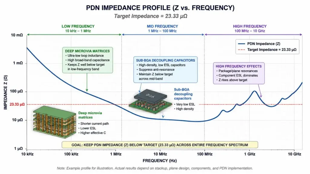
PDN Impedance Profile ($Z$ vs. Frequency) showing the $23.33~\mu\Omega$ target impedance threshold under a 1000A transient current step challenge, optimized via deep microvia matrices and sub-BGA decoupling capacitors
Hitting a micro-ohm target impedance requires stacking multiple 2oz or 3oz internal power/ground planes right next to signal tracks to minimize loop inductance (L_loop) and implementing ultra-dense deep microvia matrices for sub-BGA decoupling capacitors.
2. Core Technical Differences Driving AI PCB Engineering
A. SerDes Rate Leap: 112G PAM4 to 224G PAM4

Cross-section microscopic view comparing traditional copper foil roughness with next-generation low-profile copper foil at 56 GHz Nyquist frequency, demonstrating the mitigation of the skin effect and attenuation in 224Gbps PAM4 channels.
At 224Gbps PAM4, the Nyquist frequency climbs to an astonishing 56 GHz. At this frequency, the skin depth of copper contracts to approximately δ ≈ 0.27 μm. This means the signal travels almost exclusively through the outer roughness profile of the copper trace, rendering conventional copper treatments unusable.
- Insertion Loss Constraints: Standard high-speed FR4 or mid-loss materials exhibit attenuation values that destroy 224G signals within a few inches. AI boards require next-generation extreme low-loss (ELL) material systems such as Panasonic Megtron 8 or Tachyon 100G, which maintain a Dielectric Constant (Dk) below 3.0 and a Dissipation Factor (Df) under 0.0012 at high frequencies.
- The Channel Length Compression Crisis: Total channel loss margins for PCIe Gen6 or NVLink 5 architectures cap total insertion loss around -32dB to -36dB at Nyquist. Because of this, line lengths on the PCB copper traces are structurally limited to 4 to 5 inches. Beyond this distance, hardware architectures must shift from standard PCB traces to specialized, ultra-low-loss twinaxial overpass cables routed directly above the board to preserve signal integrity.
B. Interconnect Architecture and High-Density Breakout
Modern AI backplanes rely on high-density interconnect fabrics like NVLink or PCIe Gen6/Gen7 to synchronize large GPU arrays. To support these short-reach, high-speed architectures, traditional edge routing layouts transition into ultra-short, dense electrical breakout zones interfacing with high-density vertical/horizontal high-speed copper connectors, minimizing parasitic capacitance and cross-talk at the BGA escape area.
C. Layer Counts and Structural Complexity
To breakout thousands of signal lines from large BGA packages while providing clean power and shielding, AI boards commonly utilize 32 to over 68 layers. This requires complex sequential lamination processes.
Production Floor Note — Fabrication Director, Shenzhen Hongda Circuit Technology Co., Ltd.:
“Fabricating a 56-layer or 68-layer board is a masterclass in materials control. We utilize a 3x or 4x sequential lamination process, where sub-assemblies are laminated, drilled, plated, and then laminated again with fresh outer layers. The critical challenge is the cumulative thermal budget of the resin system; every press cycle risks resin recession, inner-layer pad shifting, and registration misalignment. Our production line utilizes advanced CCD-guided layer-to-layer registration systems to hold tolerances within ≤±1.5 mils.”
D. Copper Thickness and Power Integrity (PI)
A standard high-speed server PCB typically uses 1oz (35µm) copper for inner signal/power layers. An AI baseboard, by contrast, requires 2oz (70µm) to 3oz (105µm) copper layers dedicated to the Power Delivery Network to minimize continuous I²R DC drop. With sub-0.75V cores, an unoptimized DC voltage drop of just 12-15mV across the power plane can cause an ASIC to malfunction. To stabilize this network, high-density decoupling capacitors must be mounted directly underneath the BGA shadow on the bottom side of the board. This requires a dense matrix of deep, small-diameter blind and buried microvias to minimize loop inductance (L_loop).
E. Thermal Management Domination
With individual accelerator modules drawing 700W to 1200W+, localized heat fluxes quickly exceed air-cooling capacities. Thermal design dictates the layout of the board from day one.
- Thermal Via Arrays: AI PCBs feature massive thermal via matrices placed directly under thermal pads, filled with high-thermal-conductivity epoxy (10 W/mK to 30 W/mK) and capped with planar copper plating (POHV – Via-in-Pad Plating).
- Embedded Copper Coins: For high-stress hotspots, solid blocks of oxygen-free copper (Copper Coins) are embedded directly into the multilayer structure during lamination. This provides a direct, solid metallic path from the component package down to the cold plate or liquid-cooling manifold, bypassing the higher thermal resistance of the fiberglass resin matrix.
F. High-Density Packaging and Advanced HDI
Large AI processors use massive BGA packages with more than 5,000 to 8,000 pins, with pin pitches shrinking down to 0.8mm, 0.65mm, or finer. To safely route signals out from these dense pin arrays, designers must implement a hybrid stackup combining Any-Layer High-Density Interconnect (HDI) structures with modified Semi-Additive Processes (mSAP) in the localized breakout zones. Ultraviolet laser drills create microvias under 75µm in diameter, allowing fine line and space routing down to 25µm/25µm to ensure clean impedance matching through the inner rows of the BGA layout.
3. Shifts in Design Methodology
Design practices must shift from isolated, linear board layouts to highly integrated, multi-domain system co-designs. This requires simultaneous simulation across the chip, package, and PCB board levels.
In traditional high-speed workflows, chip packaging design and board layout were handled independently. For AI hardware, the silicon substrate, the silicon interposer, the IC packaging substrate, and the system PCB form a single, interconnected system. Engineers must perform system-level co-simulations spanning Signal Integrity (SI), Power Integrity (PI), Thermal behavior, and Mechanical warp. If an engineer runs an SI simulation without incorporating the localized heating profile, the calculated insertion loss will be inaccurate. Dielectric loss and conductor resistance both increase with temperature. At 56 GHz, a 30°C spike in localized operating temperature can cause a channel to fail its error-margin checks, destabilizing the entire system.
4. Manufacturing Bottlenecks and Yield Realities
- Sequential Lamination Shift: During sequential lamination, internal layers are subjected to temperatures above 200°C under 400 PSI of pressure multiple times. This repeated thermal cycling causes the internal resin materials to expand and contract, which can lead to inner-layer registration shifts. For a 68-layer board with a 4-mil pad diameter, a layer-to-layer alignment shift of just ±1.5 mils can cause a drill bit to clip an inner-layer ground plane, ruining the entire panel.
- High-Aspect-Ratio Plating: With total board thicknesses reaching 4.5mm to 6.0mm and through-hole drill diameters hovering around 0.25mm, the aspect ratio easily exceeds 16:1 or 20:1. Forcing liquid copper plating chemistry through these deep, narrow channels to achieve a uniform 1-mil copper wall thickness requires advanced pulse-reverse electroplating equipment and specialized wetting agents. Any thin spots or voids in the copper plating will break under the thermal stress of operational workloads.
- Fiberglass Weave Skew: Traditional glass fabrics have noticeable gaps between individual glass bundles. When high-speed differential signals run over these uneven patterns, one line of the pair may sit primarily over a glass bundle, while the other sits over resin. This imbalance creates a phase shift (skew) that destroys signal integrity at 112G and 224G speeds. To prevent this, factories must use specialized, uniformly spread-glass weaves (e.g., 1067 or 1078 styles) paired with low-profile copper foils, which significantly increases raw material costs.
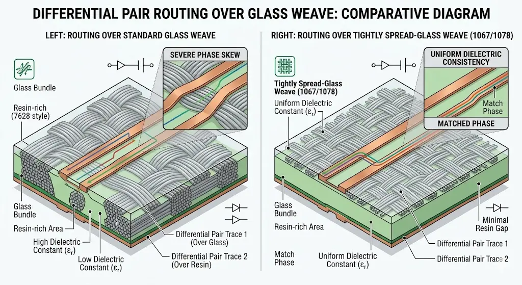
Comparative cross-section analysis of differential pair routing, illustrating how standard glass fabrics induce severe phase skew at 112G/224G, and how tightly spread-glass weaves (1067/1078 styles) restore uniform dielectric constant (Er) and phase matching.
5. Quality & Reliability Validation Benchmarks
To ensure long-term structural integrity under extreme thermal cycling, production panels are validated against rigorous international reliability benchmarks:
- Lead-Free Reflow Simulation: All high-layer count boards undergo 6x lead-free reflow testing up to 260°C without any internal delamination or microvia separation.
- Thermal Shock Resistance: Panels are subjected to 1000+ cycles of thermal shock testing (from -55°C to +125°C) to guarantee zero micro-fracturing in high-aspect-ratio plated through-holes.
- CAF Resistance: Accelerated Conductive Anodic Filamentation (CAF) testing is maintained at 85°C / 85% relative humidity for 1000 hours under a 100V bias to prevent internal electrochemical migration failures.
Frequently Asked Questions (FAQ)
Why can’t standard ultra-low-loss materials like Megtron 6 support 224Gbps PAM4 signaling over standard lengths?
At the 56 GHz Nyquist frequency of 224Gbps PAM4, Megtron 6 exhibits too high a dissipation factor (Df ≈ 0.002), which causes excessive insertion loss. Additionally, its standard fiberglass weave introduces phase skew. 224Gbps designs require next-generation materials like Megtron 8 or Tachyon 100G (Df ≤ 0.0012) paired with flat, spread-glass fabrics to maintain signal integrity over usable routing distances.
How does an AI PCB manage the thermal expansion mismatch (CTE) caused by high layer counts during assembly?
Stacking 40 to 68 layers creates mismatched expansion rates between the Z-axis of the resin and the copper vias. To prevent fracturing or trace tearing during 260°C lead-free reflow, board fabricators must select high-Tg (glass transition temperature >180°C) materials with low Z-axis thermal expansion coefficients (<2.5% expansion from 50°C to 250°C) and specify heavy anchoring pads on all internal un-functional pads.
Why is 48V power distribution preferred over traditional 12V inputs on AI accelerator baseboards?
Delivering 1200W of power at 12V requires 100A of input current, which causes significant I²R power losses and requires massive power planes. Stepping up to 48V drops the input current to 25A. Since power loss scales with the square of the current (P_loss = I²R), using 48V reduces distribution losses by roughly 16x, allowing for thinner, more efficient power plane designs.
What role does HDI technology (mSAP) play in AI boards compared to standard server boards?
Standard server boards typically use subtractive etching for traces, which caps resolution around 75µm lines and spaces. AI ASIC/GPU packages feature pin pitches below 0.8mm, requiring narrower trace widths to route signals safely between pins. Modified Semi-Additive Processing (mSAP) plates copper onto thin seed layers, allowing precise 25µm lines with straight vertical walls, ensuring clean impedance matching for high-density breakout zones.
Can simulation tools alone guarantee the first-pass success of a 68-layer AI PCB?
No. While advanced 3D electromagnetic and thermal solvers are critical, they rely on idealized material models. Real-world variations—such as resin compression, copper thickness tolerances after etching, and microvia plating shapes—introduce performance deviations. Successful first-pass manufacturing requires tight collaboration with the fabrication facility to calibrate simulation tools with actual factory test and coupon results.
Conclusion: Bringing AI-Grade Discipline to Standard PCBs
Navigating the line between cutting-edge innovation and cost-effective mass production shouldn’t be a compromise. At [PCBKR / Hongda Circuit Technology], we bridge this gap by reshaping how everyday hardware is built.
Using top-tier AI server PCB equipment to manufacture traditional PCBs delivers a strategic advantage: interlayer alignment tolerance shrinks from ±75μm to within ±25μm, and differential impedance control tightens to ±5%. Paired with 100% 3D X-Ray inspection, it grants conventional boards chip-level precision, superb signal stability, and near-100% yield.
Our Strategic Partnership to You:
We proudly stand as a strategic partner who possesses the top-tier technical ceiling of the industry’s mega-factories, yet retains the exceptional flexibility and unmatched cost-efficiency required for mid-sized, standard board campaigns. You get zero-defect reliability without paying a premium for tier-1 bureaucracy.
Ready to upgrade your hardware’s reliability?
Submit your Gerber files today for an agile engineering review and a highly competitive quote.
📧 Contact our experts: sales@pcbkr.com
About Author
David Chen https://www.linkedin.com/in/pcbcoming
David Chen boasts an extensive professional background in PCBA manufacturing, PCBA testing, and PCBA optimization, with specialized expertise in high-precision PCBA fault analysis and rigorous PCBA reliability testing. The author has worked with high-layer-count server PCB fabrication, ultra-low-loss backplane stackups, and thermo-mechanical reliability optimization for AI infrastructure projects involving 112G and 224G PAM4 architectures. Skilled in complex circuit design and cutting-edge advanced PCB manufacturing processes, he delivers solutions that elevate product durability and performance across industrial applications. His technical articles focusing on PCBA manufacturing workflows and testing methodologies are widely cited by industry peers, research institutions, and technical platforms, solidifying his reputation as a recognized technical authority in the global circuit board manufacturing sector.
2026 Shenzhen Hongda Circuit Technology Co., Ltd. | All Rights Reserved. Dedicated to High-Density, High-Compute Interconnect Infrastructures.