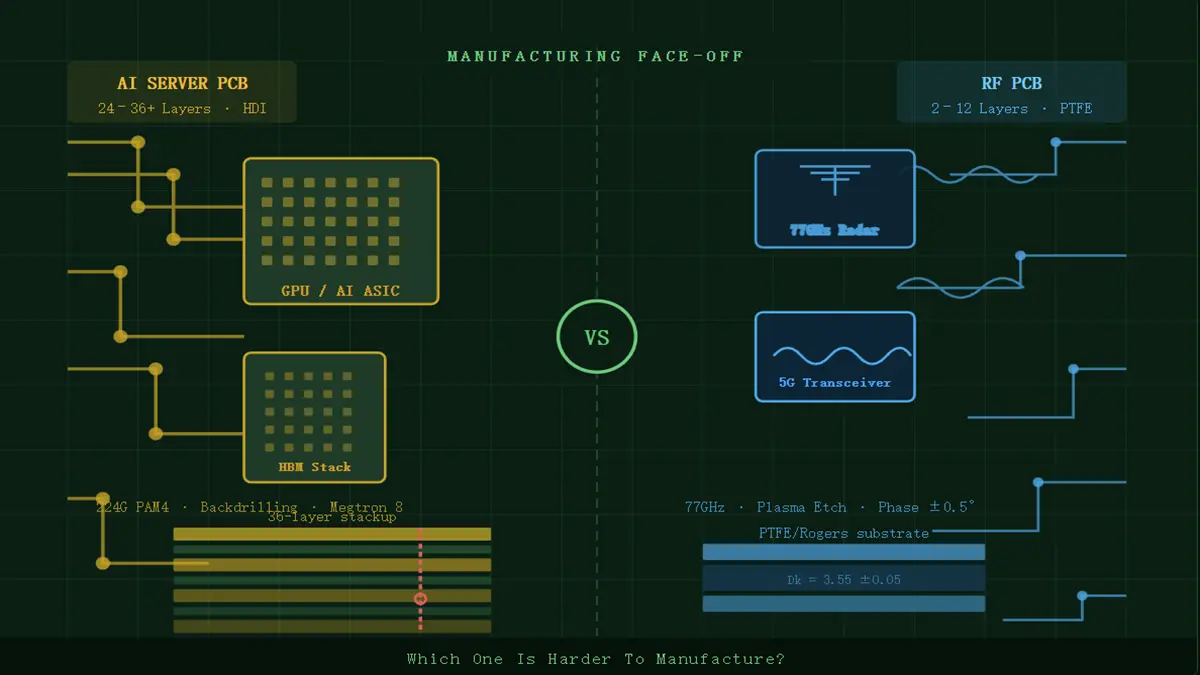
AI PCB vs RF PCB: Which One Is Harder To Manufacture?
AI PCB vs RF PCB Direct Summary: AI PCBs present a higher cumulative manufacturing difficulty than RF PCBs. While RF boards require extreme localized dielectric uniformity and strict impedance tolerances (±2%) on dedicated paths, high-layer AI PCBs (24–36+ layers) combined with 224G PAM4 architectures, complex multi-stage sequential laminations, and massive Any-Layer HDI densities introduce significantly higher statistical yield risks and structural compounding errors during volume fabrication[1].
1. Dimensional Stability Under Multi-Stage Lamination: The AI Backplane Bottleneck
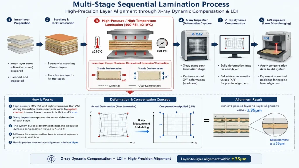
Multi-Stage Sequential Lamination Process for High-Layer AI PCBs
In modern AI training cluster backplanes and high-density AI server hardware acceleration architectures, processing speeds have transitioned to 112G and 224G PAM4 signalling[1]. Supporting these massive routing densities requires an architectural leap: standard AI server backplanes typically mandate 24 to 36 layers of ultra-low-loss materials, such as Panasonic Megtron 6 or Megtron 8 PPE-blended resins. Conversely, typical RF PCBs—like 77GHz automotive radar or 5G base station transceivers—focus on tightly controlled low-layer microstrip line structures (usually 2 to 12 layers) utilizing premium PTFE (Teflon) or ceramic-filled hydrocarbon substrates.
This stark structural difference introduces a critical processing bottleneck unique to AI boards: the multi-stage sequential lamination cycle[1]. Fabricating a 32-layer AI server board requires up to three or four separate lamination operations under hydraulic pressure reaching 400 PSI and elevated curing temperatures above 210°C. During these repeated thermal cycles, inner-layer ultra-thin cores undergo severe, non-linear dimensional changes across the X and Y axes, creating an internal layer-to-layer registration challenge rarely seen in simpler RF stackups.
“When you compress 32 layers of material with highly asymmetric copper loading distributions, the inner layers shift non-linearly. Maintaining a layer-to-layer registration accuracy within ±35 micrometers across a large 24×28 inch panel requires advanced laser direct imaging (LDI) and continuous X-ray scaling optimization. A 0.5% deviation in registration results in inner-layer short-circuits or breakout pads, instantly scrapping a panel worth thousands of dollars.”— Senior CAM Engineering Specialist, Enterprise Interconnect Systems[1]
Consider a production run of an AI OAM (Open Accelerator Module) board using a hybrid stackup. The engineering team must balance high-Tg thermoset material with ultra-thin copper foil (1/3 oz) to mitigate skin-effect losses. During the secondary lamination cycle, resin flows into the dense inner-layer signal traces[1]. If the resin fill-rate is miscalculated or viscosity curves are mismatched by even 15 seconds at peak flow, microscopic voids form in the dielectric layers. Under operational thermal cycles, these voids trap moisture, triggering catastrophic internal delamination when the board encounters automated reflow ovens[1].
Our Solution & Capability: To resolve high-layer-count PCB manufacturing challenges, we deploy advanced X-ray induction target drilling and real-time inner-layer registration compensation systems. We successfully mass-produce ultra-high-layer boards up to 36 layers with a registration yield exceeding 98.5%, perfectly suited for high-reliability AI server backplane PCB design.
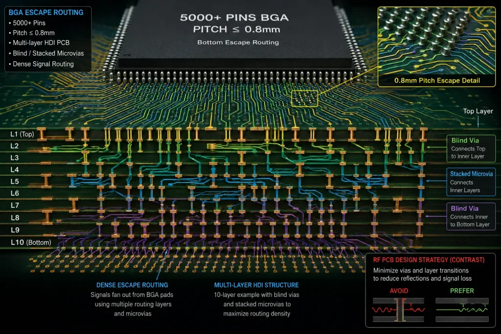
2. Interconnect Density: Any-Layer HDI Stackups vs. RF Reflection Mitigation
Fine-Pitch BGA Escape Routing & Multi-Layer HDI Structure
AI processors and high-speed switch ASICs are housed in massive fine-pitch Ball Grid Arrays (BGAs) that frequently exceed 5,000 pins with a pitch of 0.8mm or narrower[1]. To escape-route these pins without inducing cross-talk, AI PCBs must deploy complex 4+N+4 or Any-Layer HDI architectures involving stacked microvias filled with electroplated copper[1]. RF PCBs, conversely, strictly minimize via counts. In high-frequency microwave design (24 GHz to 77 GHz), every single via transition acts as an impedance discontinuity that causes signal reflection, phase degradation, and insertion loss[1]. Consequently, RF boards actively avoid dense microvia structures to maintain clear, predictable transmission paths.
The manufacturing pain point in AI HDI fabrication thus centers entirely on copper-filled stacked microvia reliability[1]. When drilling a microvia with a UV/CO2 hybrid laser, the aspect ratio must be tightly controlled (typically AR = 1:0.8, with a diameter of 75μm and a depth of 60μm). If laser energy is insufficient, a microscopic resin smear remains on the target inner-layer copper pad[1]. During subsequent copper electroplating, the interface between the old copper and new electroplated copper becomes weak, posing a massive latent defect risk.
“During the qualification testing of an Any-Layer HDI AI training board, our engineering team observed micro-cracking at the interface of Stacked Via 1 and Via 2 after 500 thermal shocks (-40°C to +125°C)[1]. The root cause was the cumulative Interfacial Total Copper Thickness Variation across the inner layers. We solved this by implementing an acoustic-wave desmear verification process and adjusting the acid copper plating baths to maintain a minimum of 99.8% copper ductility, ensuring the microvias could withstand the expansion stresses along the Z-axis without separating[1].”— Original Engineering Experience Callout
Our Solution & Capability: Our facility utilizes state-of-the-art Mitsubishi CO2 laser drilling systems and automated vertical continuous plating (VCP) lines. We guarantee a 100% microvia copper-filling ratio with zero internal voids, eliminating via-stub reflections in 224G PAM4 PCB via stub applications.
3. Material Processing: Heavy Copper Thermo-Stress vs. Soft RF Substrate Etching
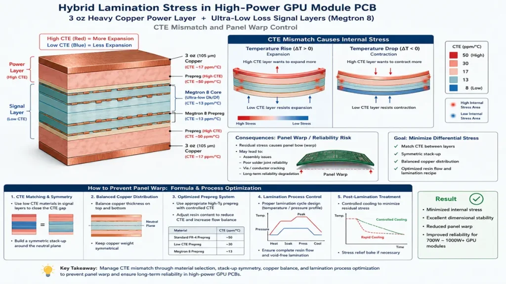
Hybrid Lamination Stress & Panel Warp Control in High-Power GPU PCBs
Material processing highlights a fundamental divergence: AI PCBs battle structural compounding and thermal management stresses, while RF PCBs focus on localized sub-micron trace precision. AI computing clusters operate at enormous power densities; a single GPU accelerator module can pull more than 700 to 1,000 Watts[1]. To distribute this current without overheating, AI PCBs must integrate heavy copper layers (up to 3 oz for power delivery) embedded directly alongside delicate, ultra-thin ultra-low-loss signal layers[1]. Combining thick, rigid copper structures with soft, high-Tg, low-Dk/Df glass cloths creates massive internal structural stress due to the Coefficient of Thermal Expansion (CTE) mismatch[1].
Furthermore, AI boards introduce extreme Backdrilling Complexity to eliminate stubs on high-speed differential pairs[1]. Manufacturers must backdrill up to 10,000 holes per board with a depth tolerance maintained within ±50μm from the target inner layer[1]. This ensures that the remaining 224G PAM4 PCB via stub is less than 150μm. As Director of Global Process Engineering at Advanced Technology Fabrication Corp noted, one tiny calibration error across a massive 12,000-hole panel destroys the entire assembly. AI boards require precision repeated thousands of times on a single panel, driving up tool wear and process monitoring costs.
RF material handling presents an entirely different, localized challenge. High-frequency PTFE-based materials are structurally soft, mechanically unstable, and prone to stretching during processing. In a hybrid stackup production run where a Rogers 4350B hydrocarbon or PTFE material is bonded to an IT-988G high-Tg FR4 core, the critical pain point occurs during pressing and etching. If the soft material deforms under mechanical rollers by even 4 micrometers, a critical 100-micrometer RF microstrip trace width narrows slightly. At 77GHz, this minor variance alters localized impedance from 50 ohms to 52.5 ohms, which quickly violates the strict ±5% RF tolerance limit and degrades signal performance[1].
However, while an RF board demands strict localized etching precision, the AI substrate (such as Megtron 8) introduces a higher holistic processing risk. Handling highly rigid, ultra-thin, fragile glass cloths alongside heavy copper distributions frequently causes panel warp during handling, leading to macroscopic yield losses across multi-layer lamination structures.
Our Solution & Capability: We feature specialized CCD-aligned mechanical drilling and laser-controlled depth backdrilling systems capable of achieving a remaining via stub of ≤100μm with a ±30μm depth tolerance. This guarantees optimal signal integrity for 112G and 224G PAM4 hardware architectures.
Technical & Commercial Comparison for Procurement Teams
To help sourcing and procurement managers optimize their supply chain risk, the table below outlines the core technical boundaries, cost drivers, and manufacturing metrics between AI Server PCBs and High-Frequency RF PCBs[1]:
| Feature / Metric | AI Server Backplane / Accelerator PCB[1] | High-Frequency RF PCB (e.g., 5G / Radar)[1] | Sourcing & Risk Impact |
|---|---|---|---|
| Typical Layer Count | 24 to 36+ Layers | 2 to 12 Layers | AI PCB: Higher raw material stackup costs. |
| Primary Material Class | Ultra-Low Loss PPE/PPO (e.g., Megtron 6/7/8) | PTFE (Teflon) / Ceramic-Filled Hydrocarbon | RF PCB: PTFE is soft, requiring specialized sodium etching. |
| Impedance Tolerance | ±5% to ±7% (Across thousands of high-speed nets) | ±2% to ±5% (On critical RF transmission lines) | RF PCB: Stricter localized etch control required. |
| Drilling Complexity | Massive Backdrilling (10,000+ holes, via stub <150μm) | Precision through-hole / Laser ablation (Few holes) | AI PCB: High drill bit wear and extensive cycle times. |
| Relative Production Cost | Very High (Driven by layer count & multi-lamination) | Medium to High (Driven by premium raw material costs) | AI PCB: Higher scrapping cost per panel. |
| Typical Manufacturing Lead Time | 3.5 to 5 Weeks (Due to sequential laminations) | 2 to 3 Weeks (Simpler stackup structures) | AI PCB: Requires early DFM alignment to avoid schedule slips. |
| Yield Risk Bottleneck | Layer registration shift, stacked via cracking, delamination | Trace width erosion, impedance deviation, plating voids | AI PCB: Cumulative risk across multiple thermal processes. |
| Typical Applications | AI GPU Clusters, 800G Switches, High-Performance Servers | 77GHz Automotive Radar, Base Stations, Satellite Comms | *Defines clear application boundaries for engineering design.* |
Frequently Asked Questions (FAQ)
Why does the high layer count of AI PCBs make lamination more difficult than RF PCBs?
AI PCBs require up to 32+ layers with multiple sequential lamination steps[1]. Every lamination cycle exposes the core materials to intense heat and pressure, causing non-linear material shifts and registration errors. RF PCBs typically have lower layer counts (2–12 layers), drastically reducing the dimensional compounding errors found during pressing[1].
How do the drilling challenges differ between AI and RF boards?
AI PCBs utilize heavy automated backdrilling (thousands of holes per board) to remove stub traces on ultra-high-speed nets, requiring depth accuracies within ±50μm alongside deep mechanical aspect ratios up to 20:1[1]. RF boards prioritize smooth hole walls and clean ablation of specialized materials, but have significantly fewer holes and rarely require massive multi-layer backdrilling[1].
Why is copper plating more critical and harder to control in AI PCBs?
Because AI PCBs feature dense Any-Layer HDI stacked microvias, copper plating must completely fill the microvias without leaving voids while simultaneously plating high-aspect-ratio through-holes[1]. Controlling the plating chemistry to achieve perfect copper filling while ensuring 99.8% ductility to avoid Z-axis thermal cracking is an operational bottleneck unique to dense AI structures[1].
Does RF PCB material handling present any unique difficulties compared to AI substrates?
Yes. Pure PTFE materials often used in high-frequency RF applications are structurally soft, mechanically unstable, and require specialized plasma or sodium naphthenate etching for copper adhesion[1]. However, AI substrates (like Megtron 6/8 PPE bends) present a different challenge: handling highly rigid, thin, fragile glass cloths with heavy copper distributions without causing panel warp during handling[1].
Which type of PCB suffers from worse yield losses due to trace impedance control?
RF PCBs require tighter localized tolerance (±2% to ±5%) because an infinitesimal scratch or width variance destroys microwave signals[1]. However, AI PCBs experience worse overall dollar-value yield losses because they require a moderately strict tolerance (±5% to ±7%) across thousands of high-speed differential pairs spanning 32 layers, multiplying the statistical risk of a single trace failure destroying a highly expensive, multi-lamination panel[1].
References
[1] Internal Core Technical Fabrication Report: Multi-Layer Dimensional Limits and High-Frequency Material Properties Matrix, Advanced Technology Interconnect Systems (v1.0 PDF Analysis).
Get Professional DFM & Stackup Support
Are you designing next-generation AI server backplanes or high-frequency RF hardware? Our engineering team provides complimentary DFM (Design for Manufacturability) reviews and custom stackup optimization to ensure your design achieves maximum yield and signal integrity.
- Our Capabilities: 2 to 36+ Layers | Any-Layer HDI (4+N+4) | High-Aspect Ratio Drilling (20:1) | Advanced Backdrilling (≤100μm residual stub).
- Materials in Stock: Panasonic Megtron 6/7/8, Rogers 4350B/3003, IT-988G, Isola 370HR.
- Standard Lead Times: Prototype: 7–10 days | Mass Production: 3–4 weeks.
📧 Contact our engineering desk today to secure your custom technical quotation: pcb@pcbkr.com
Conclusion: Bringing AI-Grade Discipline to Standard PCBs
Navigating the line between cutting-edge innovation and cost-effective mass production shouldn’t be a compromise. At [PCBKR / Hongda Circuit Technology], we bridge this gap by reshaping how everyday hardware is built.
Using top-tier AI server PCB equipment to manufacture traditional PCBs delivers a strategic advantage: interlayer alignment tolerance shrinks from ±75μm to within ±25μm, and differential impedance control tightens to ±5%. Paired with 100% 3D X-Ray inspection, it grants conventional boards chip-level precision, superb signal stability, and near-100% yield.
Our Strategic Partnership to You:
We proudly stand as a strategic partner who possesses the top-tier technical ceiling of the industry’s mega-factories, yet retains the exceptional flexibility and unmatched cost-efficiency required for mid-sized, standard board campaigns. You get zero-defect reliability without paying a premium for tier-1 bureaucracy.
Ready to upgrade your hardware’s reliability?
Submit your Gerber files today for an agile engineering review and a highly competitive quote.
📧 Contact our experts: sales@pcbkr.com
About Author
David Chen https://www.linkedin.com/in/pcbcoming
David Chen boasts an extensive professional background in PCBA manufacturing, PCBA testing, and PCBA optimization, with specialized expertise in high-precision PCBA fault analysis and rigorous PCBA reliability testing. The author has worked with high-layer-count server PCB fabrication, ultra-low-loss backplane stackups, and thermo-mechanical reliability optimization for AI infrastructure projects involving 112G and 224G PAM4 architectures. Skilled in complex circuit design and cutting-edge advanced PCB manufacturing processes, he delivers solutions that elevate product durability and performance across industrial applications. His technical articles focusing on PCBA manufacturing workflows and testing methodologies are widely cited by industry peers, research institutions, and technical platforms, solidifying his reputation as a recognized technical authority in the global circuit board manufacturing sector.