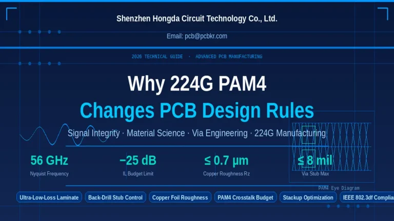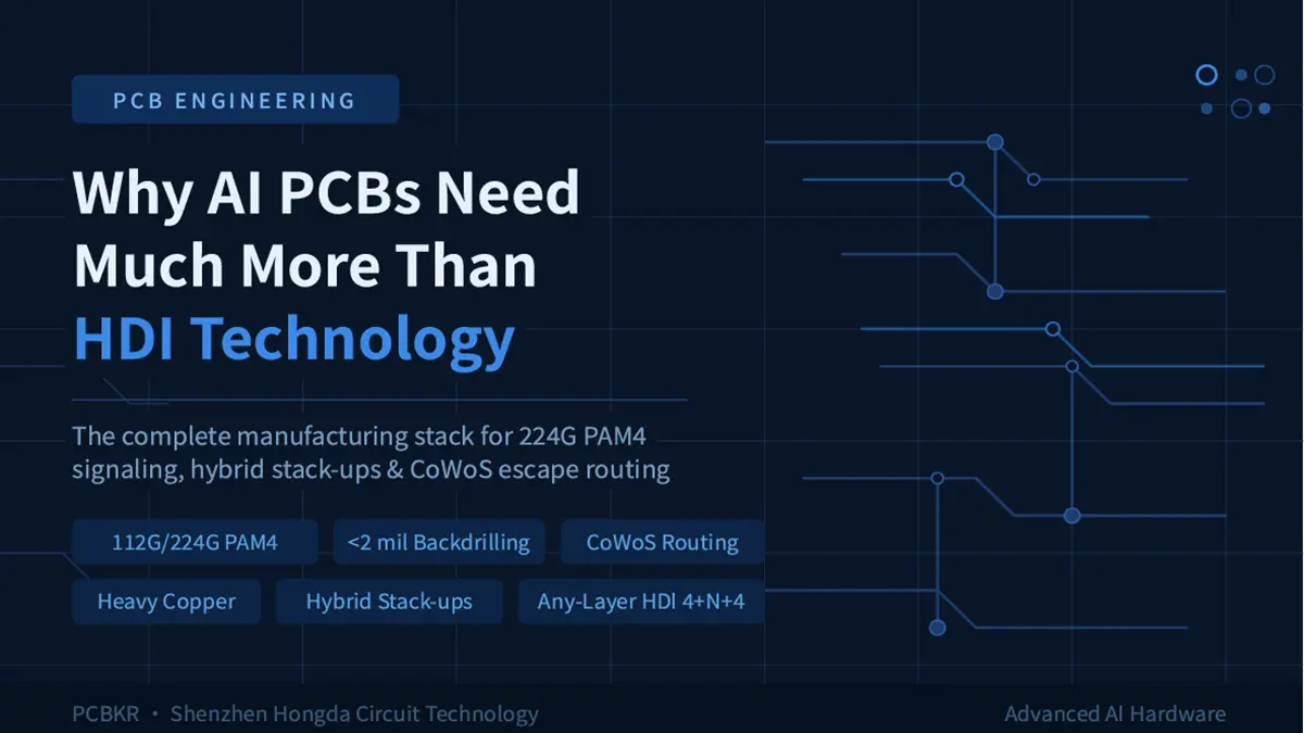
Why AI PCBs Need Much More Than HDI Technology
Introduction: The Quantitative Realities of AI Hardware
Many procurement managers and hardware designers operate under a significant misconception: they assume an AI Printed Circuit Board (PCB) is merely an upgraded High-Density Interconnect (HDI) board[cite: 1]. While HDI is necessary for routing high-density component footprints, it represents less than 30% of the entire system engineering matrix required for modern AI infrastructure[cite: 1].
Treating an AI GPU baseboard or OAM (Open Accelerator Module) as a standard high-density digital board inevitably triggers severe signal integrity (SI) degradation, power delivery bottlenecks, and catastrophic thermal runaway. At next-generation data rates, traditional PCB manufacturing margins do not just shrink—they completely vanish.
The System-Level Definition of an AI PCB
AI clusters rely on massively parallel computing architectures that operate under extreme physical constraints. Unlike standard networking hardware, AI hardware applications must manage unique electrical and mechanical baselines[cite: 1]:
- GPU Accelerator Modules (OAMs): Accommodating high-wattage silicon architectures requiring localized power transmission networks and sub-0.4mm pitch escape boundaries[cite: 1].
- AI Server Backplanes / UBB (Universal Baseboards): Interconnecting multiple 700W–1000W+ compute nodes via ultra-low-latency physical channels[cite: 1].
- High-Speed Fabric Switch Boards: Handling immense East-West traffic densities across scale-out architectures[cite: 1].
These environments force layer counts to climb between 24 to 48 layers, utilizing complex material stack-ups engineered to sustain 112G and 224G PAM4 signaling speeds[cite: 1]. At these frequencies, the PCB can no longer be treated as a passive interconnection substrate; it must be manufactured as a tuned, high-frequency wave-guiding system.
Why HDI Technology Alone Fails at 112G/224G
HDI technology leverages microvias, stacked configurations, and fine line-space routing to maximize pin breakout density[cite: 1]. However, scaling the microvia structure alone cannot resolve the primary electromagnetic and thermodynamic bottlenecks encountered in AI hardware:
1. The Stub Resonance Problem
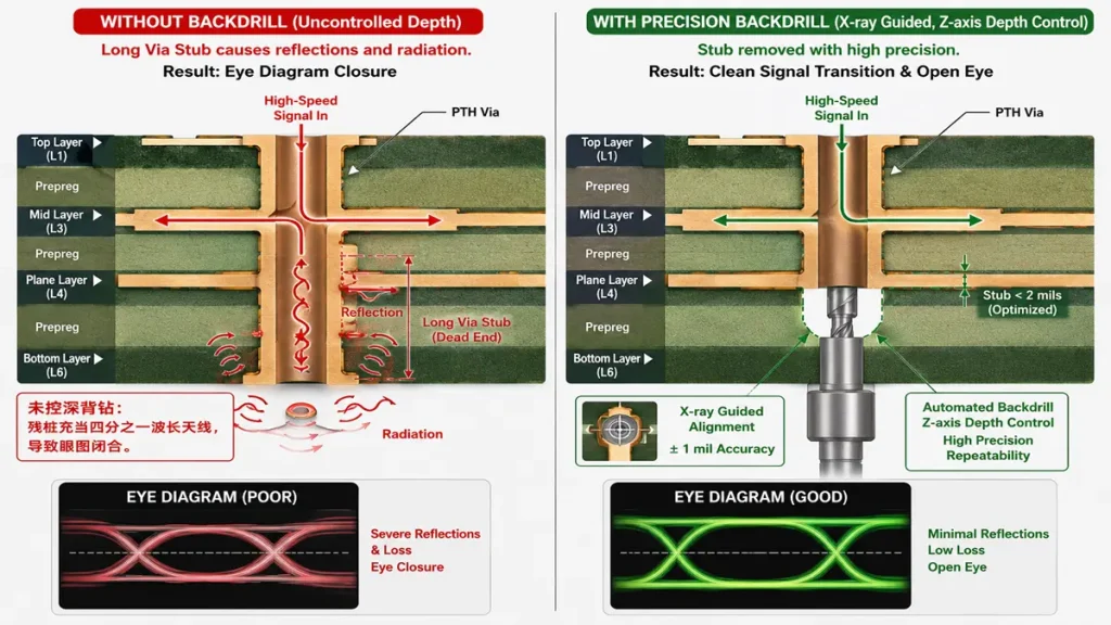
Comparative Analysis of High-Precision Backdrilling vs. Uncontrolled Via Stub Resonance in 224G PAM4 AI PCBs
HDI layout strategies still rely on standard plated through-hole (PTH) vias for vertical layer transitions across thick multi-layer structures. Any unused vertical portion of a PTH via creates a “via stub”[cite: 1]. At 224G PAM4, a via stub longer than 5 mil (0.127mm) acts as a quarter-wave resonant antenna, generating severe signal reflections, crushing the eye diagram, and driving Bit Error Rates (BER) beyond acceptable system limits[cite: 1].
2. Dielectric Losses Across Extended Trace Lengths
While HDI manages local component escape routing efficiently, it cannot mitigate insertion loss along the long differential trace paths (often exceeding 12 to 20 inches) found in massive AI server chassis[cite: 1]. Standard HDI materials introduce unacceptable attenuation at Nyquist frequencies of 28 GHz (for 56G NRZ/112G PAM4) and 56 GHz (for 224G PAM4).
3. Power Integrity (PI) and IR Drop Limitations
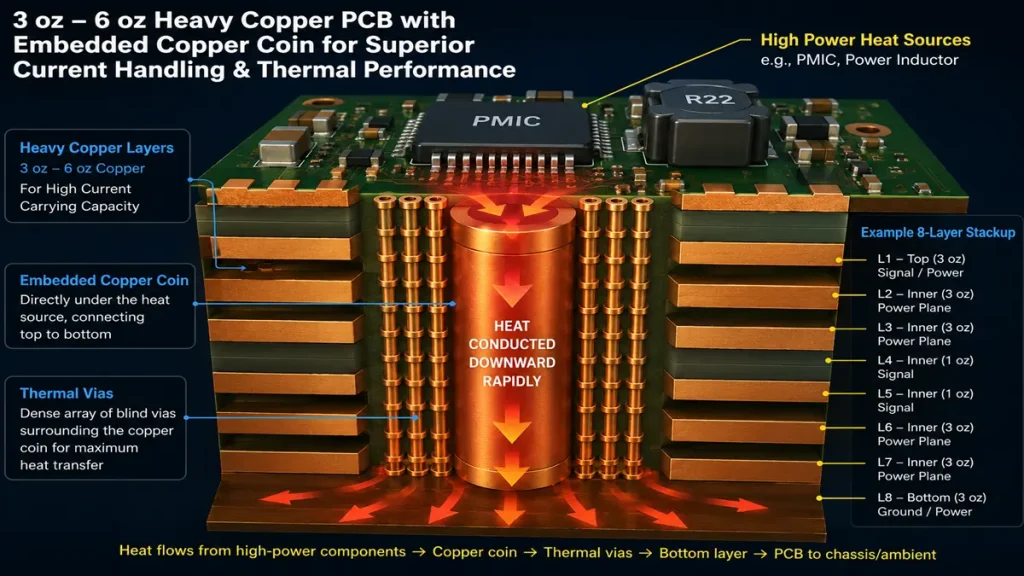
3oz – 6oz Heavy Copper PCB Structure with Embedded Copper Coin and Thermal Vias for AI Hardware Power Delivery
Standard HDI builds typically utilize thin copper foils (0.5 oz or 1 oz) to achieve fine line/space geometries. Modern AI accelerators draw dynamic currents exceeding 1000A at sub-1.0V core voltages. Thin copper structures cannot handle these loads, resulting in severe IR Drop (voltage drop), local DC resistance heating, and power rail voltage fluctuations that destabilize the ASIC core.
The Advanced Manufacturing Stack Required for AI Infrastructure
To fabricate a functionally stable AI hardware platform, a manufacturer must tightly integrate a suite of specialized, high-tolerance fabrication processes alongside traditional HDI capabilities[cite: 1]:
| Advanced Process Technology | Quantitative Target / Engineering Objective | Primary System Benefit |
|---|---|---|
| Precision Controlled-Depth Backdrilling | Remaining target stub length: < 2 mils (0.05mm) with ±1 mil depth accuracy. | Eliminates high-frequency via stub resonance at 56 GHz Nyquist frequencies[cite: 1]. |
| Ultra-Low Loss (ULL) Glass/Resin | Df (Dissipation Factor) ≤ 0.0012 and Dk (Dielectric Constant) ≤ 3.0 at 10GHz–30GHz. | Minimizes insertion loss across long channel backplanes (e.g., Megtron 8, Tachyon 100G)[cite: 1]. |
| Hybrid Material Stack-up Lamination | Asymmetric registration control with layer-to-layer alignment tolerance of ≤ ±3 mils (0.075mm). | Combines ULL materials for high-speed layers with standard FR-4 for power/ground to optimize cost and structural stability. |
| Heavy Copper Embedded Layers | Inner and outer copper thickness up to 3 oz – 6 oz on power distribution layers. | Sustains >1000W power distribution networks while mitigating IR Drop and thermal dissipation bottlenecks[cite: 1]. |
| Embedded Copper Coins & Thermal Vias | Direct metal-to-metal bonding; thermal conductivity up to 390 W/m•K. | Conducts high-density localized heat away from localized Power Management ICs (PMICs)[cite: 1]. |
Advanced Packaging (CoWoS) and Escape Routing Challenges
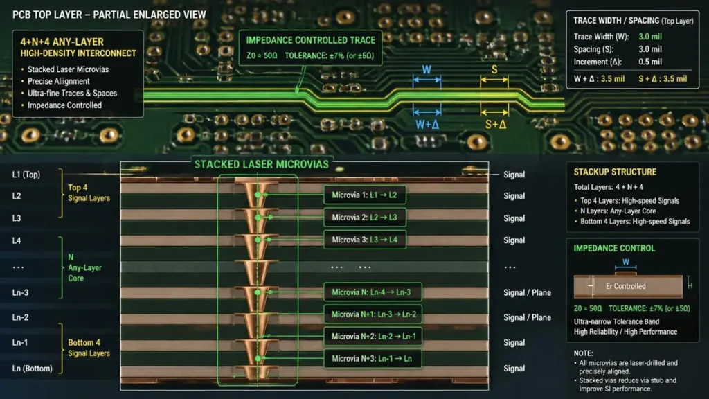
4+N+4 Any-Layer HDI Stackup and Stacked Laser Microvia Cross-Section with Tight Impedance Control
The routing challenges of modern AI baseboards are directly driven by semiconductor advanced packaging. Silicon configurations like CoWoS (Chip-on-Wafer-on-Substrate) integrate high-bandwidth memory (HBM3e/HBM4) and compute chiplets onto an intermediate substrate, resulting in extreme pin counts with BGA pitches reduced to 0.4mm or 0.35mm.
To successfully navigate this congestion without introducing catastrophic capacitive crosstalk, manufacturers must utilize Any-Layer HDI structures (up to 4+N+4 configurations) using ultra-precise stacked laser microvias[cite: 1]. This layout allows signal escape paths to drop vertically through the board immediately, bypassing traditional routing bottlenecks[cite: 1]. However, this density demands that copper trace width and spacing tolerances be maintained strictly within ±10% to ensure predictable 50Ω single-ended and 85Ω/100Ω differential impedance profiles.
The Reality of Via Stub Removal: Advanced Backdrilling
At 224G PAM4 signaling, the mechanical margin for error is virtually zero[cite: 1]. The diagram below contrasts a standard PTH via transition with an advanced backdrilled configuration required for AI signals[cite: 1]:
[Option A: Standard PTH Configuration]        [Option B: High-Precision Backdrill]
         (Signal Degraded)                              (Signal Optimized)
              |---|                                           |---|
==============|===|============== Top Layer  =================|===|============== Top Layer
              |   |                                           |   |
  ============|===|============ Layer 6 (SIG)   ==============|===|============ Layer 6 (SIG)
              |   |                                           |   |
              |   | [Critical Failure]                        |___| <-- Target Stub < 2 mils
==============|===|============== Bottom Layer                |   |
              |---| (Unused Stub Acts As                      |   | <-- Air Gap / Resins Filled
                     a Resonant Antenna)                      |___|
To ensure structural integrity and signal performance across a 32-layer AI baseboard, fabricators must implement automated X-ray registration control alongside dynamic, Z-axis controlled-depth drilling systems[cite: 1]. A stub remaining even slightly over specification can compromise the entire channel’s performance.
Evaluating High-Layer Count Hybrid Backplanes
AI cluster backplanes present unique manufacturing challenges because they physically link multiple heavy server chassis together[cite: 1]. These boards frequently exceed thicknesses of 4.0mm to 6.0mm, maintaining aspect ratios greater than 16:1[cite: 1].
When laminating these extreme layer counts using heterogeneous materials (such as pairing Panasonic Megtron 8 with Isola mid-loss materials), the differing coefficients of thermal expansion (CTE) introduce significant internal stress. Without optimized lamination cycles and precise temperature ramping profiles, the board will suffer from inner-layer delamination, microvia shearing, or wrap-around plating failures during automated assembly reflow cycles.
Strategic Technical Criteria for AI PCB Vendor Evaluation
Sourcing partners cannot rely on general commercial PCB manufacturing baselines when qualifying suppliers for AI infrastructure hardware[cite: 1]. Procurement teams must verify the following manufacturing benchmarks:
- Advanced Registration Tolerances: Capability to maintain layer-to-layer registration within ≤ ±3 mils across a 30+ layer stack-up during high-pressure lamination.
- Advanced Drilling Control: Production-level deployment of dual-sided X-ray guided backdrilling capable of hitting < 2 mil remaining stubs consistently.
- Impedance Accuracy: Ability to guarantee tighter-than-standard trace impedance control (±5Ω or ±7% tolerance boundaries) across ultra-low loss laminates.
- In-House DFM and SI/PI Simulation: Front-end engineering teams equipped to run pre-production signal and power integrity simulation verification to cross-check stack-up designs.
Conclusion: System Engineering Defines Yield
Ultimately, high-performance AI PCB fabrication cannot be achieved through standalone technologies like HDI[cite: 1]. It represents an interconnected system engineering problem where routing density, signal fidelity, power delivery networks, and thermodynamic stress must be co-optimized simultaneously[cite: 1]. Successful deployment relies on early collaboration between the design team and a fabricator capable of executing tight mechanical tolerances and advanced process integrations.
Optimize Your AI Hardware: Get a Complimentary Engineering DFM Review
Navigating the physical realities of 224G PAM4 signaling, 32+ layer hybrid stack-ups, and extreme thermal dynamics requires an experienced fabrication partner. Shenzhen Hongda Circuit Technology Co., Ltd. (PCBKR) delivers the advanced manufacturing capabilities needed to move your complex high-speed designs from layout to successful hardware deployment.
- Our Capabilities: 24 to 48-Layer Backplanes, Any-Layer HDI, Precision Backdrilling (stubs < 2 mil), Heavy Copper (up to 6 oz), and full SI/PI Simulation Support.
- Material Logistics: Certified and stable access to Panasonic Megtron 6/8, Isola Tachyon 100G, and Doosan ultra-low loss laminates.
- Quality Standards: AS9100D, ISO9001, IATF16949, and UL certified production lines.
Eliminate manufacturing risks before releasing your design. Submit your preliminary stack-up parameters or Gerber files to our technical engineering division at sales@pcbkr.com today for a comprehensive, non-disclosure-backed DFM review and technical evaluation.
Frequently Asked Questions (FAQ)
Why can’t standard Any-Layer HDI satisfy 224G PAM4 routing requirements for AI hardware?
While Any-Layer HDI provides excellent local routing density for fine-pitch BGAs (0.4mm or smaller), it focuses strictly on component fan-out, not high-frequency signal mechanics. At 224G PAM4 (56 GHz Nyquist frequency), any tiny geometric discontinuity—such as an un-backdrilled via stub or a ±15% impedance fluctuation—causes catastrophic signal reflection and insertion loss. AI hardware requires a system-level integration of Any-Layer HDI combined with dual-sided precision backdrilling (stubs < 2 mil) and ultra-low-loss laminates like Megtron 8 to maintain eye diagram closure.
What is the maximum acceptable via stub length for 112G and 224G AI server PCBs?
For 112G PAM4, the remaining via stub must be tightly controlled under 5 mils (0.127mm). For next-generation 224G PAM4, the mechanical margin drops to virtually zero, demanding a target stub length of < 2 mils (0.05mm) with a drilling depth accuracy of ±1 mil. Any stub exceeding this threshold acts as a quarter-wave resonant antenna, generating severe resonance notches that corrupt the high-frequency channel’s Bit Error Rate (BER).
How do manufacturers handle the thermal and power demands of 1000W+ AI GPUs on a single board?
Sourcing a reliable AI PCB requires evaluating the fabricator’s heavy copper and thermal management capabilities. To sustain a Power Distribution Network (PDN) drawing >1000A at sub-1.0V core voltages, fabricators must embed 3 oz to 6 oz heavy copper layers to eliminate IR Drop. Thermally, standard vias are inadequate; the board must integrate high-density thermal via arrays or direct-bonded embedded copper coins (offering thermal conductivity up to 390 W/m·K) beneath localized Power Management ICs (PMICs) to conduct intense heat away from the silicon.
What material selection challenges arise when designing 32+ layer hybrid AI backplanes?
High-layer-count AI backplanes (often 4.0mm to 6.0mm thick) require a Hybrid Material Stack-up to balance performance and cost—layering Ultra-Low Loss (ULL) laminates (e.g., Panasonic Megtron 8 or Isola Tachyon 100G) on high-speed lines with mid-loss FR-4 on ground/power planes. The core challenge is managing different Coefficients of Thermal Expansion (CTE). Without precise lamination pressure cycles and optimized temperature ramping profiles, the board will suffer from inner-layer delamination or microvia shearing during assembly reflow.
What technical benchmarks should a procurement manager use to qualify an AI PCB supplier?
Standard HDI qualification checklists are insufficient for AI hardware. Procurement managers must explicitly audit four advanced technical benchmarks:
1.Layer-to-layer registration tolerance: Must consistently hit ≤ ±3 mils (0.075mm) across a 30+ layer hybrid stack-up.
2.Backdrilling capability: Production-level validation of dual-sided X-ray guided depth control capable of hitting < 2 mil stubs.
3.Impedance control boundaries: Ability to guarantee ultra-tight trace impedance tolerances within ±5Ω or ±7%.
4.Advanced Packaging Experience: Proven track record of handling routing escape layouts for CoWoS (2.5D/3D) advanced packaging formats.
About Author
David Chen https://www.linkedin.com/in/pcbcoming
David Chen boasts an extensive professional background in PCBA manufacturing, PCBA testing, and PCBA optimization, with specialized expertise in high-precision PCBA fault analysis and rigorous PCBA reliability testing. The author has worked with high-layer-count server PCB fabrication, ultra-low-loss backplane stackups, and thermo-mechanical reliability optimization for AI infrastructure projects involving 112G and 224G PAM4 architectures. Skilled in complex circuit design and cutting-edge advanced PCB manufacturing processes, he delivers solutions that elevate product durability and performance across industrial applications. His technical articles focusing on PCBA manufacturing workflows and testing methodologies are widely cited by industry peers, research institutions, and technical platforms, solidifying his reputation as a recognized technical authority in the global circuit board manufacturing sector.