What PCB Technologies Are Used in AI Data Centers?
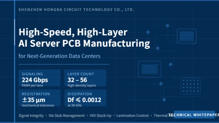
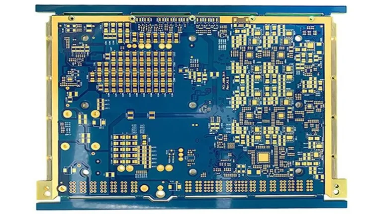
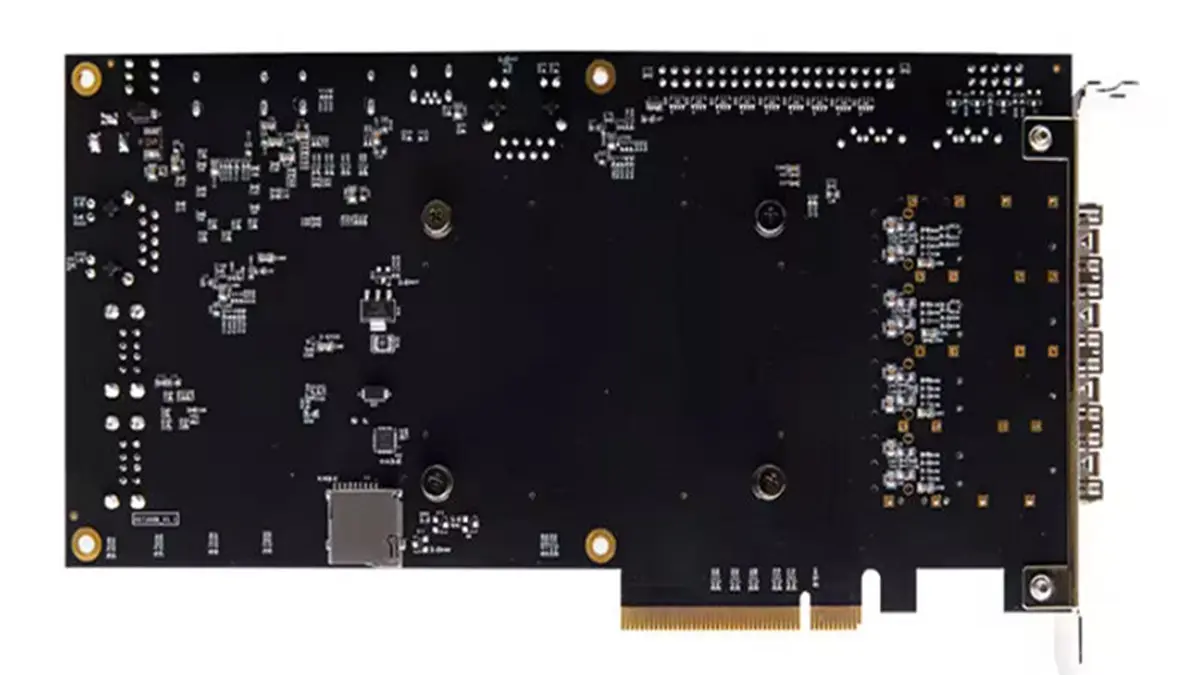
AI data centers rely on ultra-high-layer-count PCBs, low-loss materials, HDI structures, advanced backdrilling, high-current copper designs, and 112G/224G PAM4 architectures to support GPU clusters exceeding 800G networking bandwidth and 1000A power delivery requirements.
Why Do AI Data Centers Require Completely Different PCB Technologies?
AI data center PCBs operate under dramatically higher bandwidth, current density, and thermal stress conditions than traditional enterprise servers. Conventional FR4-based server boards cannot reliably support modern AI accelerator platforms using 112G PAM4, PCIe Gen5/Gen6, NVLink, and 800G optical networking.
| Parameter | Traditional Server | AI Data Center Server |
|---|---|---|
| Total Board Power | 300–500W | 3–8kW |
| Typical Layer Count | 8–14 Layers | 20–36 Layers |
| Signal Speed | 10–25Gbps | 56G/112G/224G PAM4 |
| Current Delivery | <300A | 800–1200A+ |
Manufacturing Pain Point: In real AI server production, PCB bottlenecks increasingly originate from copper current spreading and thermal expansion behavior rather than traditional logic routing limitations.
Senior signal integrity engineers frequently describe AI server PCBs as a hybrid of telecom backplanes, RF systems, and high-current power electronics. That characterization is accurate because AI boards must simultaneously solve insertion loss, impedance stability, via resonance, and thermal fatigue issues.
Why Are Ultra-Low-Loss Materials Mandatory in AI Server PCBs?
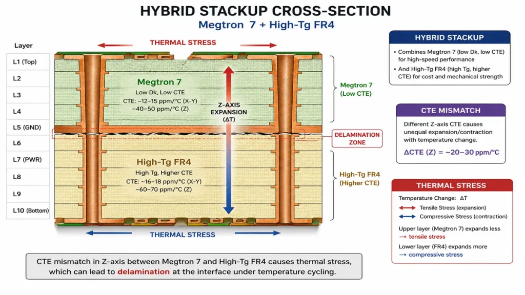
HYBRID STACKUP CROSS-SECTION: Megtron 7 + High-Tg FR4
Standard FR4 materials generate excessive insertion loss and phase instability at 112G PAM4 frequencies. AI data center PCBs therefore require ultra-low-loss laminates such as Megtron 6, Megtron 7, and Tachyon materials.
| Material | Dk @10GHz | Df @10GHz | Application |
|---|---|---|---|
| Standard FR4 | 4.1–4.5 | 0.015–0.020 | Traditional Servers |
| Megtron 6 | 3.4 | 0.002 | 112G AI Systems |
| Megtron 7 | 3.30 | 0.0012 | 224G Development |
When operating at 28GHz Nyquist frequency for 56GBaud/112G PAM4 and 56GHz Nyquist frequency for 112GBaud/224G PAM4, standard ultra-low-loss glass cloth styles such as 1078 or 1067 e-glass generate severe fiber-weave skew effects. To suppress skew and insertion loss instability, AI server PCBs increasingly mandate HVLP or RTF copper profiles with average surface roughness targets below Rz ≤ 1.2μm or Ra ≤ 0.25μm.
Under 85% relative humidity stress testing, even Megtron 7 can experience dielectric loss degradation approaching 25% if open-weave glass styles are improperly selected. At these frequencies, humidity absorption becomes a measurable signal integrity variable rather than merely a material reliability concern.
Manufacturing Pain Point & Engineering Fix: In a 32-layer hybrid stackup alternating Megtron 7 and High-Tg FR4 power layers, the severe Z-axis CTE mismatch created massive internal stress accumulation. Megtron 7 exhibited a post-Tg CTE-Z near 38ppm/°C, while High-Tg FR4 exceeded 55ppm/°C. During the third lead-free reflow cycle at 260°C, inner-layer delamination appeared directly at the hybrid material boundary. Our engineering fix introduced a Gradient Curing Profile by extending the lamination dwell time at 210°C from 60 minutes to 95 minutes under tightly controlled 380psi pressure, while adding a 0.5-mil organo-silane high-bond adhesion treatment on internal copper surfaces to improve interfacial reliability.
In one 28-layer AI accelerator fabrication project, cumulative material movement after multiple lamination cycles caused layer registration drift approaching 75μm, despite high-end drilling equipment remaining within specification.
Why Do AI Data Center PCBs Use Extremely High Layer Counts?
AI accelerator boards require extremely high layer counts because routing density, power integrity, shielding, and signal isolation requirements exceed the capabilities of conventional server stackups.
| Platform | Typical Layer Count |
|---|---|
| Traditional Enterprise Server | 8–14 Layers |
| GPU Accelerator Carrier Board | 20–28 Layers |
| AI Training Baseboard | 26–36 Layers |
| 800G Switch Backplane | 30–40+ Layers |
Modern AI boards allocate dedicated routing regions for PAM4 channels, HBM escape routing, ground shielding, retimer pathways, clock isolation, and heavy copper power planes.
Manufacturing Pain Point: As layer count rises above 30 layers, sequential lamination accuracy and drill registration become yield-critical. Even micron-scale movement can destroy microvia capture alignment.
Why Is HDI Technology Essential for AI Accelerator Boards?
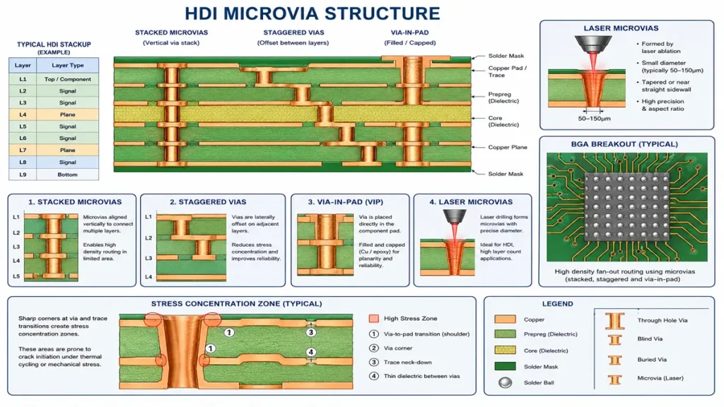
HDI PCB Microvia Structure: Stacked, Staggered, and Via-in-Pad Designs
AI GPUs and switch ASICs use ultra-fine-pitch BGAs that cannot be routed using traditional through-hole PCB technology. HDI structures enable sufficient breakout density and signal escape routing.
| HDI Technology | Purpose |
|---|---|
| Laser Microvias | Fine-Pitch Routing |
| Stacked Microvias | High Routing Density |
| Staggered Vias | Improved Reliability |
| Via-in-Pad | BGA Escape Optimization |
Next-generation AI ASICs increasingly adopt 0.8mm and even 0.6mm BGA pitch architectures containing more than 8,500 pins. Conventional mechanically drilled vias with 0.2mm hole diameters fail due to aspect-ratio limitations and routing congestion. AI server boards therefore migrate from ELIC 3+N+3 structures toward advanced 4+N+4 HDI architectures.
Laser microvias are commonly drilled at 75μm (3mil) diameters targeting 225μm (9mil) pads, leaving a maximum total registration tolerance window of only ±25μm across a massive 24 × 18-inch production panel.
Chief Signal Integrity Architect’s Directive: “When routing 112G PAM4 lines beneath the BGA area, you cannot afford fully stacked microvias from Layer 1 down to Layer 4. The accumulated stress at the interface between the Layer 2 and Layer 3 copper joints creates an unpredictable structural bottleneck under 100% computational workloads. If the copper plating thickness within the laser microvia is uneven—even by as little as 3μm—the localized current crowding will trigger an interfacial separation. For long-term AI hardware survivability, staggered configurations with an offset of at least 150μm are mandatory.”
Manufacturing Pain Point: Repeated thermal cycling during AI workloads accelerates stacked microvia fatigue, leading to barrel cracking, interfacial separation, and copper fatigue failures.
Reliability engineers increasingly favor staggered microvia designs over fully stacked architectures for long-duration AI training clusters operating continuously at high utilization.
Why Is Backdrilling Critical for 112G/224G PAM4 AI Systems?
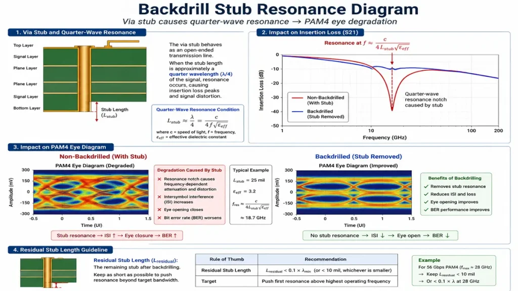
Backdrill Stub Resonance Mechanism and Its Impact on PAM4 Signal Integrity
Backdrilling removes unused via stubs that otherwise behave as resonant structures at ultra-high frequencies, severely degrading PAM4 signal integrity.
| Signaling Standard | Typical Residual Stub Target |
|---|---|
| 25G NRZ | <10 mil |
| 56G PAM4 | <6 mil |
| 112G PAM4 | <4 mil |
| 224G PAM4 | <2–3 mil |
For 112G PAM4 signaling, via stubs exceeding 10mil (0.254mm) generate quarter-wave resonance notches near the 28GHz Nyquist frequency, causing insertion loss spikes larger than −4.5dB. At 224G PAM4 speeds, the maximum allowable residual stub target must remain strictly below 2mil (0.05mm).
AI backplanes often exceed 3.5–5.5mm thickness with more than 30 layers, making precision backdrilling extraordinarily difficult.
Real Production Failure Scenario: During validation of a 4.2mm thick AI OAM board, conventional mechanical backdrilling produced residual stub variation ranging from 3mil to 8mil. This inconsistency caused 12% of differential pairs to fail the 3.0dB COM specification. The root cause involved combined stack-thickness tolerance variation (±10%) and local warp across the large-format panel.
Engineering Fix: The production line abandoned traditional contact-depth drilling and upgraded to CCD-controlled laser depth sensing combined with Dynamic Z-axis Real-time Mapping. By mapping coordinate heights across a 50 × 50mm grid prior to drilling, the residual stub variance was tightened to a verifiable ≤1.5mil across all 14,000 backdrilled holes per board.
Why Do AI Server PCBs Require Heavy Copper Structures?
Modern AI GPUs consume massive power levels requiring extremely low-impedance power delivery networks capable of handling 800–1200A transient current loads.
| GPU Generation | Approximate Power |
|---|---|
| Traditional GPU | 250–300W |
| Modern AI Accelerator | 700–1200W |
| Future AI Platforms | 1500W+ |
Modern AI OAM modules increasingly demand up to 1,200A core current while operating below 0.8V. To maintain IR drop below 15mV, internal power planes require 3oz (105μm) or 4oz (140μm) copper layers embedded between high-speed signal layers.
This massive copper concentration near the VRM region creates severe thermal gradients, with localized temperatures exceeding 135°C during sustained large-language-model training workloads.
Manufacturing Pain Point & Engineering Fix: Embedding 3oz copper inside ultra-high-layer-count boards creates severe resin starvation risks. Standard prepregs such as 106 or 1080 lack sufficient resin content to fully fill the dense spacing between heavy copper structures, resulting in microscopic voids and long-term CAF reliability risks. Our production solution implemented a Resin Fill Optimization Strategy using high-resin-content prepregs such as 2116 HR with nearly 70% resin content positioned directly adjacent to heavy copper planes. The vacuum cycle was also modified to maintain ≤5 Torr vacuum pressure for 45 minutes before hydraulic compression.
In one 32-layer AI compute platform investigation, redistributing copper density reduced total board warp from 1.8mm to 0.6mm across a large-format panel.
Why Is Thermal Reliability More Dangerous in AI PCBs?
AI systems operate continuously at extremely high utilization and thermal density levels, accelerating copper fatigue, dielectric degradation, CAF formation, and solder reliability risks.
- VRM hotspots may exceed 120°C
- Connector hotspots may exceed 105°C
- HBM regions experience concentrated thermal loading
- Localized via field heating becomes common
Real AI Failure Scenario: One AI training cluster repeatedly crashed after 10 hours of operation. The root cause was eventually traced to temperature-induced dielectric expansion altering differential impedance and collapsing PAM4 eye margins.
FAQ:
What is the biggest difference between AI PCBs and traditional server PCBs?
AI PCBs must simultaneously support ultra-high bandwidth, massive current delivery, advanced thermal management, and extreme signal integrity performance.
Why are low-loss materials necessary for AI servers?
Because standard FR4 cannot maintain acceptable insertion loss and phase stability at 112G and 224G PAM4 frequencies
Why are AI server PCBs so expensive?
They require ultra-low-loss laminates, HDI structures, high layer counts, sequential lamination, heavy copper designs, precision backdrilling, and extremely tight manufacturing tolerances.
Why is PCB warpage dangerous in AI systems?
Warped boards can damage BGA solder reliability, connector alignment, and long-term thermal stability in GPU accelerator platforms.
Why will 224G PAM4 make AI PCB manufacturing harder?
224G PAM4 dramatically reduces signal margin tolerance, requiring even lower insertion loss, shorter via stubs, tighter impedance control, and better material consistency.
Using top-tier AI server PCB equipment to manufacture traditional PCBs delivers a strategic advantage: interlayer alignment tolerance shrinks from ±75μm to within ±25μm, and differential impedance control tightens to ±5%. Paired with 100% 3D X-Ray inspection, it grants conventional boards chip-level precision, superb signal stability, and near-100% yield.
Still, need help? Contact Us: sales@pcbkr.com
Need a PCB or PCBA quote? Quote now
About Author
David Chen https://www.linkedin.com/in/pcbcoming/
David Chen boasts an extensive professional background in PCBA manufacturing, PCBA testing, and PCBA optimization, with specialized expertise in high-precision PCBA fault analysis and rigorous PCBA reliability testing. Skilled in complex circuit design and cutting-edge advanced PCB manufacturing processes, he delivers solutions that elevate product durability and performance across industrial applications. His technical articles focusing on PCBA manufacturing workflows and testing methodologies are widely cited by industry peers, research institutions, and technical platforms, solidifying his reputation as a recognized technical authority in the global circuit board manufacturing sector.